Victor G. Karpov - Physics of Thin-Film Photovoltaics
Здесь есть возможность читать онлайн «Victor G. Karpov - Physics of Thin-Film Photovoltaics» — ознакомительный отрывок электронной книги совершенно бесплатно, а после прочтения отрывка купить полную версию. В некоторых случаях можно слушать аудио, скачать через торрент в формате fb2 и присутствует краткое содержание. Жанр: unrecognised, на английском языке. Описание произведения, (предисловие) а так же отзывы посетителей доступны на портале библиотеки ЛибКат.
- Название:Physics of Thin-Film Photovoltaics
- Автор:
- Жанр:
- Год:неизвестен
- ISBN:нет данных
- Рейтинг книги:4 / 5. Голосов: 1
-
Избранное:Добавить в избранное
- Отзывы:
-
Ваша оценка:
Physics of Thin-Film Photovoltaics: краткое содержание, описание и аннотация
Предлагаем к чтению аннотацию, описание, краткое содержание или предисловие (зависит от того, что написал сам автор книги «Physics of Thin-Film Photovoltaics»). Если вы не нашли необходимую информацию о книге — напишите в комментариях, мы постараемся отыскать её.
Many concepts here fall beyond the classical PV scope. The differences lie in device thinness (microns instead of millimeters) and morphology (non-crystalline instead of crystalline). In such structures, the charge carriers can reach electrodes without recombination. On the other hand, thin disordered structures render a possibility of detrimental lateral nonuniformities (“recombination highways”), and their energy spectra give rise to new recombination modes. The mechanisms of thermal exchange and device degradation are correspondingly unique.
The overall objective of this book is to give a self-contained in-depth discussion of the physics of thin-film systems in a manner accessible to both researchers and students. It covers most aspects of the physics of thin-film PV, including device operations, material structure and parameters, thin-film junction formation, analytical and numerical modeling, concepts of large area effects and lateral non-uniformities, physics of shunting (both shunt growth and effects), and device degradation. Also, it reviews a variety of physical diagnostic techniques proven with thin-film PV. Whether for the veteran engineer or the student, this is a must-have for any library.
Physics of Thin-Film Photovoltaics — читать онлайн ознакомительный отрывок
Ниже представлен текст книги, разбитый по страницам. Система сохранения места последней прочитанной страницы, позволяет с удобством читать онлайн бесплатно книгу «Physics of Thin-Film Photovoltaics», без необходимости каждый раз заново искать на чём Вы остановились. Поставьте закладку, и сможете в любой момент перейти на страницу, на которой закончили чтение.
Интервал:
Закладка:
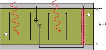
Fig. 4 In thin film devices, drift rather than diffusion can determine the kinetics of photogenerated carriers. They readily arrive at the corresponding electrodes avoiding interactions with recombination centers. Having reached the electrodes they can move to the entrances of rare but highly efficient recombination channels shorting between the electrodes and playing the role of recombination highways.
As illustrated in Fig. 5, spatial separation of charge carriers at GB can significantly decrease the probability of their recombination compared to crystalline materials where electrons and holes are distributed uniformly. That creates a possibility for polycrystalline thin film PV to potentially outperform their crystalline counterparts. On the other hand, high concentration of impurities and defects in the grain boundary interfaces enhances the recombination processes, which can make grain boundaries detrimental and polycrystalline material PV devices perform worse than crystalline PV. The latter feature was evidenced in some polycrystalline Si structures. Furthermore, it will be shown below ( Sec. XVI) that the very nature of recombination processes in non-crystalline materials can be significantly different from that dominating crystalline PV and affecting both the GB and main junction processes. Overall, the role of grain boundaries remains debatable and material/recipe specific with experiments exhibiting either beneficial or detrimental GB effects. It is possible that some of GBs in thin films form, with certain probability, much more effective recombination channels than others. Those channels can play the role of recombination highways depicted in Fig. 4.
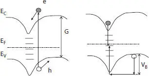
Fig. 5 Role of grain boundaries in noncrystalline thin film PV. Left: Sketch of the electron hole pair creation by a photon of energy exceeding the forbidden gap G . E cand E vare conduction and valence band edges, E Fis the Fermi energy. Short horizontal lines represent defect states located at the grain boundary. Note that the positive (attractive to electrons) GB charge is assumed arbitrarily. For the case of negative GB charge, the potential well (barrier) for electrons (holes) will turn into a barrier (well). Right: the GB barrier requires charge carrier activation [with probability proportional to exp(− V B/ kT )] which suppresses recombination (presented by vertical arrows).
A physically nontrivial and practically important property of thin film PV (further discussed in Sec. V) is that, under certain conditions, they exhibit thermal runaway instabilities favored by low heat transfer parameters as well as low sheet resistances along with significant currents and voltages. These instabilities result in local (~ 1 mm) spots of elevated temperature that can degrade PV performance and trigger nonuniform structure damage. We will discuss later their underlying physics and factors that can be tweaked to mitigate the latter detrimental effects by proper device engineering.
A more specific structure of the two major brands, CdTe and CIGS based thin film PV is presented in Fig. 6. It is understood that in reality the glass is facing up in CdTe cells. The CdTe and CIGS layers are absorbers responsible for the light conversion into photogenerated electrons and holes. The question of their doping has been debatable for decades, with extreme views ranging from that these materials cannot be effectively doped to that of beneficial or detrimental role of certain impurities. Many of such mutually exclusive points have found experimental confirmations with particular device recipes.
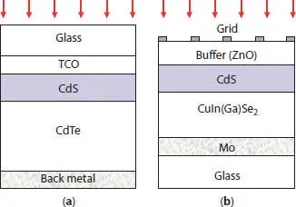
Fig. 6 A cross-sectional view of a superstrate (glass sheet up) CdTe based and substrate (glass sheet down) CIGS based thin film solar cell (not to scale). The CdTe cell front contact is formed by the transparent conductive oxide (TCO). The typical layer thicknesses are 2-4 μm for CdTe and CIGS, 0.1-0.2 μm for CdS, 0.5 μm for TCO and buffer layer, 0.1-0.2 μm for back metal (Mo for CIGS), 1-3 mm for glass. The drawing does not show the polycrystalline structure of CdTe, CIGS, and CdS layers. Red arrows represent incident sunlight.
Furthermore, the role of CdS layer often found with CdTe and CIGS remained mysterious long after it was empirically found to be extremely important and practically irreplaceable in spite of its lack of contribution to photocurrent. We shall see in what follows ( Sec. XVIII) that its piezo-electric properties may be a key leading to piezo-photovoltaic coupling beneficial for PV operations.
Finally, the back contact layer renders yet another set of puzzles. While the Mo back contact is typical of CIGS PV, there are several successful recipes of back contact in CdTe based PV. It was found indeed that the back contact has profoundly strong effect on device operations in spite of the fact that it is not photoactive (light does not penetrate there). The so-called back barrier due to the junction field between the semiconductor and back metal turns out to be a culprit. More in detail, the physics of back contact functionality will be discussed in Sec. VB. The front contact layer, such as TCO in CdTe based PV or ZnO in CIGS, has its nontrivial properties as well, as also discussed in the subsequent chapters.
Last but not the least is the issue of thin film PV degradation. Light, elevated temperatures, and humidity can all play a detrimental role in degradation processes. Some PV companies went under being unable to solve these problems. It often happened that the most efficient PV devices exhibited the highest degradation rates calling upon tradeoffs between efficiency and stability. It should be understood that PV degradation is inevitable with any PV in full compliance with the general Le Chatelier - Brown principle stating that when a settled system is disturbed, it will adjust to diminish the change that has been made to it, or, roughly stated, any change in status quo prompts an opposing reaction in the responding system [18]. With respect to PV, that principle predicts that PV structures will evolve in such a way as to decrease the light induced electric currents; hence, degradation. While all PVs degrade, the thin film ones are especially vulnerable due to their thinness allowing formation of conductive transverse channels (shunts). In addition, thin film structures accumulate extremely high electrostatic energy density (similar to narrow gap (~ 1 μm) electric capacitors) capable of discharging with huge power dissipation transforming material structure towards electric shorts that minimize the electric energy. A more in detail discussion of these issues will be given in Sec. XXVII B.
References
1. M. A. Green, Solar Cells: Operating Principles, Technology and System Applications, Prentice Hall, Englewood Cliffs, N.J., 1982.
2. A. L. Fahrenbruch, R. H. Bube, Fundamentals of Solar Cells , Academic Press (1983).
3. J. L. Gray, The physics of Solar Cells , in Handbook of Photovoltaic Science and Engineering, p. 61, Edited by A. Lique and S. Heggedus, Wiley (2002).
4. J. Nelson, The Physics of Solar Cells , Imperial College Press (2003).
5. P. Wurfel, Physics of Solar Cells , Wiley (2005).
Читать дальшеИнтервал:
Закладка:
Похожие книги на «Physics of Thin-Film Photovoltaics»
Представляем Вашему вниманию похожие книги на «Physics of Thin-Film Photovoltaics» списком для выбора. Мы отобрали схожую по названию и смыслу литературу в надежде предоставить читателям больше вариантов отыскать новые, интересные, ещё непрочитанные произведения.


Обсуждение, отзывы о книге «Physics of Thin-Film Photovoltaics» и просто собственные мнения читателей. Оставьте ваши комментарии, напишите, что Вы думаете о произведении, его смысле или главных героях. Укажите что конкретно понравилось, а что нет, и почему Вы так считаете.