Victor G. Karpov - Physics of Thin-Film Photovoltaics
Здесь есть возможность читать онлайн «Victor G. Karpov - Physics of Thin-Film Photovoltaics» — ознакомительный отрывок электронной книги совершенно бесплатно, а после прочтения отрывка купить полную версию. В некоторых случаях можно слушать аудио, скачать через торрент в формате fb2 и присутствует краткое содержание. Жанр: unrecognised, на английском языке. Описание произведения, (предисловие) а так же отзывы посетителей доступны на портале библиотеки ЛибКат.
- Название:Physics of Thin-Film Photovoltaics
- Автор:
- Жанр:
- Год:неизвестен
- ISBN:нет данных
- Рейтинг книги:4 / 5. Голосов: 1
-
Избранное:Добавить в избранное
- Отзывы:
-
Ваша оценка:
Physics of Thin-Film Photovoltaics: краткое содержание, описание и аннотация
Предлагаем к чтению аннотацию, описание, краткое содержание или предисловие (зависит от того, что написал сам автор книги «Physics of Thin-Film Photovoltaics»). Если вы не нашли необходимую информацию о книге — напишите в комментариях, мы постараемся отыскать её.
Many concepts here fall beyond the classical PV scope. The differences lie in device thinness (microns instead of millimeters) and morphology (non-crystalline instead of crystalline). In such structures, the charge carriers can reach electrodes without recombination. On the other hand, thin disordered structures render a possibility of detrimental lateral nonuniformities (“recombination highways”), and their energy spectra give rise to new recombination modes. The mechanisms of thermal exchange and device degradation are correspondingly unique.
The overall objective of this book is to give a self-contained in-depth discussion of the physics of thin-film systems in a manner accessible to both researchers and students. It covers most aspects of the physics of thin-film PV, including device operations, material structure and parameters, thin-film junction formation, analytical and numerical modeling, concepts of large area effects and lateral non-uniformities, physics of shunting (both shunt growth and effects), and device degradation. Also, it reviews a variety of physical diagnostic techniques proven with thin-film PV. Whether for the veteran engineer or the student, this is a must-have for any library.
Physics of Thin-Film Photovoltaics — читать онлайн ознакомительный отрывок
Ниже представлен текст книги, разбитый по страницам. Система сохранения места последней прочитанной страницы, позволяет с удобством читать онлайн бесплатно книгу «Physics of Thin-Film Photovoltaics», без необходимости каждый раз заново искать на чём Вы остановились. Поставьте закладку, и сможете в любой момент перейти на страницу, на которой закончили чтение.
Интервал:
Закладка:
In general, the built-in electric fields always emerge with junctions of any two chemically different materials. The underlying physics is that one of the materials will be energetically more favorable for the electrons than the other. To minimize the system energy, the electrons will therefore move there leaving the one with unbalanced positive charge; hence, the built-in field between the spatially separated opposite charges of electrons and holes, qualitatively similar to that of electric capacitor. The number of electrons moving across the junction is determined by the balance between the above mentioned energy gain and the energy loss due to the necessity of overcoming the Coulomb attraction to the positive charges left behind. The built-in electric fields of that nature are omnipresent and are not limited to photovoltaics, or p-n junctions, or other artificial structures.
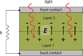
Fig. 1 Conceptual design of a solar cell. Front and back contacts are metallic, and the former one is transparent to light (shown in waving lines). The presented built-in electric field E is caused by the dark positive and negative charges shown as + and −. R is a load resistor. For specificity, the diagram presents a two semiconductor layer design, such as p- and n- materials with the field E in their junction proximity. However, sufficient electric fields can exist as well in the proximities of semiconductor-metal junctions.
Another reading of the latter statement is that photovoltaics do not necessarily have to be related to or understood in terms of p-n junctions. In reality, any (not only p-n) junctions of different materials produce built-in electric fields. Some of them, but not all, create photovoltaic effect.
For example, a junction of two metals produces the built-in field underlying the phenomenon of thermoelectricity, but not suitable for PV because the light does not penetrate in a metal deep enough and because that field is screened (by metal electrons) beyond a nanometer thin region, insufficient for light absorption. However the built-in fields of metal/semiconductor (rather than metal/metal) junctions can make good diodes and PV devices.
As another example, we point at a charge acquired by a solid particle immersed in a liquid. Curiously, that example explains how wines and many other liquid products consist of charged micro particles suspended in a somewhat ionized water. We will return to that example later in the book describing the so called “red wine effect” in PV.
Note that junction fields require electronic exchange between two materials while their direct physical contact is not necessary. As an illustration, chemically different metal electrodes of a capacitor will spontaneously acquire opposite charges proportional to the difference in their work functions. That process often called the ‘dielectric absorption’ takes time sufficient for the inter-plate electron transfer. Along the same lines, two different metals separated by a dielectric or semiconductor layer will exchange electrons forming the built-in electric field throughout that layer as described more in detail next (Sec. II).
B. Fundamental Material Requirements
A well known feature of all PV devices is that at least some of their constituting materials must have a not-too-wide forbidden gap, say G ~ 1–2 eV. The origin of that criterion is that larger band gaps exceeding the energies of most of sun spectra photons would not allow efficient light absorption necessary to produce enough electrons and holes. However, there is also the opposite requirement of those gaps being not too small, so that efficiently absorbing narrow band semiconductors are not good for PV either. As a result, semiconductors with substantial but not-too-wide forbidden gaps G ~ 1–2 eV, such as Si, Ge, CdTe, CIGS and some others are most suitable for PV.
The not-too-narrow gap limitation is less intuitive and may be worth explaining here. It is dictated by PV functionality as a power source. The power is a product of electric current and voltage, P = IV where both I and V components must be not too small. I is proportional to the light induced charge generation rate favoring significant absorption coefficients in the sun spectral region of ħω ~ 0.5–2 eV. Forbidden gaps G ~ 1–2 eV of many semiconductors fall in that region. To the contrary, the typical dielectric gaps G ≳ 4 eV are too wide for sufficient absorption (for example, window glass that is practically transparent and does not absorb light).
The requirement that undermines the suitability of narrow gap semiconductors (despite their strong absorption coefficients) is related to the voltage component: V ≤ G/q , where q is the electron charge. To explain the latter inequality we note that V can be related to the difference in Fermi energies in two metal electrodes as illustrated in Fig. 2. We recall that the Fermi (quasi-Fermi) energy describes the energy change due to removing one particle from the system. Therefore, ΔE F≡ E F1− E F2gives the energy change due to transferring one electron between the two metals, and so does qV . On the other hand, the metal Fermi energies must not overlap with the semiconductor conduction or valence bands because such an overlap would mean that the semiconductor has in reality metal conductivity (no gap between the Fermi level and forbidden gap edges). As illustrated in Fig. 2, G presents the upper limit of the difference between the electron and hole Fermi levels allowing their steady state spatial separation. Increasing V beyond G/q would shift the Fermi levels beyond the forbidden gap turning the semiconductor into metal thus shorting the built in field and the circuit.
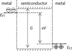
Fig. 2 Band diagram of a metal/semiconductor/metal structure where E F1and E F2represent quasi-Fermi levels determined by voltage drop V across the semiconductor.
Another wording of the same is that electrons and holes recombine very efficiently when the two Fermi levels are close thus suppressing their spatial separation and the built-in field. Assuming point defect mediated recombination, it can be shown more quantitatively [12] that the electron-hole recombination rate strongly accelerates with decrease of the gap G . As a result, there exists a range of gaps optimizing PV performance, G ≲ 2 eV. It should be remembered however, that the latter optimum gap prediction was derived under certain assumptions about the nature of (defect facilitated) recombination, lack of traps, insignificant leakage due to shunts, and others clearly outlined in the original work [12].
C. Charge Transport. Definition of Thin Film PV
We now consider charge carriers transport in the junction region where the built in field is significant; that region is often called the space charge region, simply because the field and charge density are ∇ E= 4π ρ (where Eand ρ are correspondingly the field and charge density, and we use the Gaussian system of units). The built-in field extends through a limited thickness l Edetermined by the condition that the change of electron energy through l Eequals the difference in Fermi levels ΔE Fof the materials involved. In the order of magnitude, the latter condition yields  where n is the charge concentration (cm −3) and ε is the dielectric permittivity (for simplicity, we neglect possible differences in n and ε between the junction components). Using the ballpark values, ΔE F~ 1 eV, ε ~ 10, n ~ 10 16cm −3yields l E~ 1 μm. This estimate is consistent with the published data for various junctions.
Интервал:
Закладка:
Похожие книги на «Physics of Thin-Film Photovoltaics»
Представляем Вашему вниманию похожие книги на «Physics of Thin-Film Photovoltaics» списком для выбора. Мы отобрали схожую по названию и смыслу литературу в надежде предоставить читателям больше вариантов отыскать новые, интересные, ещё непрочитанные произведения.


Обсуждение, отзывы о книге «Physics of Thin-Film Photovoltaics» и просто собственные мнения читателей. Оставьте ваши комментарии, напишите, что Вы думаете о произведении, его смысле или главных героях. Укажите что конкретно понравилось, а что нет, и почему Вы так считаете.