Victor G. Karpov - Physics of Thin-Film Photovoltaics
Здесь есть возможность читать онлайн «Victor G. Karpov - Physics of Thin-Film Photovoltaics» — ознакомительный отрывок электронной книги совершенно бесплатно, а после прочтения отрывка купить полную версию. В некоторых случаях можно слушать аудио, скачать через торрент в формате fb2 и присутствует краткое содержание. Жанр: unrecognised, на английском языке. Описание произведения, (предисловие) а так же отзывы посетителей доступны на портале библиотеки ЛибКат.
- Название:Physics of Thin-Film Photovoltaics
- Автор:
- Жанр:
- Год:неизвестен
- ISBN:нет данных
- Рейтинг книги:4 / 5. Голосов: 1
-
Избранное:Добавить в избранное
- Отзывы:
-
Ваша оценка:
Physics of Thin-Film Photovoltaics: краткое содержание, описание и аннотация
Предлагаем к чтению аннотацию, описание, краткое содержание или предисловие (зависит от того, что написал сам автор книги «Physics of Thin-Film Photovoltaics»). Если вы не нашли необходимую информацию о книге — напишите в комментариях, мы постараемся отыскать её.
Many concepts here fall beyond the classical PV scope. The differences lie in device thinness (microns instead of millimeters) and morphology (non-crystalline instead of crystalline). In such structures, the charge carriers can reach electrodes without recombination. On the other hand, thin disordered structures render a possibility of detrimental lateral nonuniformities (“recombination highways”), and their energy spectra give rise to new recombination modes. The mechanisms of thermal exchange and device degradation are correspondingly unique.
The overall objective of this book is to give a self-contained in-depth discussion of the physics of thin-film systems in a manner accessible to both researchers and students. It covers most aspects of the physics of thin-film PV, including device operations, material structure and parameters, thin-film junction formation, analytical and numerical modeling, concepts of large area effects and lateral non-uniformities, physics of shunting (both shunt growth and effects), and device degradation. Also, it reviews a variety of physical diagnostic techniques proven with thin-film PV. Whether for the veteran engineer or the student, this is a must-have for any library.
Physics of Thin-Film Photovoltaics — читать онлайн ознакомительный отрывок
Ниже представлен текст книги, разбитый по страницам. Система сохранения места последней прочитанной страницы, позволяет с удобством читать онлайн бесплатно книгу «Physics of Thin-Film Photovoltaics», без необходимости каждый раз заново искать на чём Вы остановились. Поставьте закладку, и сможете в любой момент перейти на страницу, на которой закончили чтение.
Интервал:
Закладка:
In the built-in field region, the charge carrier transport is dominated by drift with velocity v = μF where μ is the mobility and F = qE = qV/l Eis the electric force. The diffusion with coefficient D = μkT (according to the Einstein formula where k is the Boltzmann constant and T is the temperature) is insignificant contributing to the transport time a relatively small fraction of kT/qV ≪ 1 assuming the typical V ~ 1 V and kT ~ 0.025 eV (room temperature).
The drift transport approximation is sufficient if the light absorption is limited to the space charge region, which applies to many thin-film structures. That approximation is well justified when the light absorption length is short enough, l abs≲ l E, limiting charge carrier generation to the built-in field region, which takes place in CdTe, CIGS, and a variety of other thin-film PV materials. However, some crystalline structures, such as Si and Ge, possess the non-direct band structures with absorption lengths in the hundred of microns range. In such materials, charge carriers generation extends way beyond the built-in region, and the transport is dominated by diffusion rather than drift. We recall that the characteristic diffusion distance and time are related as  where D is the diffusion coefficient.
The above discussed drift and diffusion times,
(1) 
describe how long it take for a charge carrier to travel distance l to the device terminals. These times must be short enough to avoid significant electron-hole recombination. If the characteristic recombination time is τ r, we must require that the relevant transport time to device terminals, τ Eor τ Dbe shorter than τ r. The corresponding criteria are discussed in Sec. XVIbelow. Here, it suffices to note that τ ris extremely sensitive to material parameters and device structure, which brings in multiple elements of materials science and PV technology. In particular, recombination processes are strongly facilitated by structural defects (imperfections, impurities, surface states) that depend on details of material composition; interfacial recombination can play a significant role for some junctions, etc.
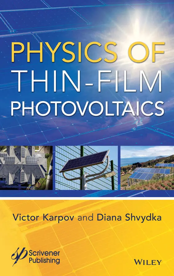
At a qualitative level, we discriminate between thick and thin PV structures. Typical of crystalline PV, the former are such that the electrons and holes diffuse long distances to the device terminals and τ Dcan be longer than τ r, i.e. interaction with defects becomes inevitable during their long trips. To the contrary, the characteristic drift time τ Eis much shorter than τ rin thin PV where recombination becomes almost immaterial. As a result, defects and imperfections determine thick PV efficiency quite significantly. That observation undisputable for thick PV, can become confusing when uncritically extended over thin film PV where it is not warranted. Furthermore, a century-long successful history of crystalline (Si, in the first place) PV made the concept of defect facilitated recombination literary a commandment dominating all PV understanding across the discipline. That paradigm has triggered various defect characterization studies in thin film structures, and, while no correlations between defects and thin film PV performances was established, that activity continues.
Of course, the difference between ‘thick’ and ‘thin’ devices is related to the fact that the former have thickness l ≫ l Ewhere l Eis the linear dimension of the built-in field region, as presented in Fig. 3. To the contrary, l ≲ l Eor l is just slightly greater than l Efor ‘thin’ devices. In the absence of field, charge carriers have to travel by diffusion. Taking into account the Einstein relation between the mobility and diffusion coefficient, the ratio of ‘thick’ over ‘thin’ device transport times is estimated as
(2) 
where V is the voltage across the device, q is the electron charge. Given the typical | Ve | ~ 1 eV, kT ~ 0.025 eV (room temperature), l on the order of hundreds of micron and l Ein microns, the ratio in Eq. (2)can be as large as 10 5–10 6. The latter inequality is consistent with the typical experimental data: the diffusion times τ d,thick~ 10–100 μ s (in crystalline Si PV) and t d~ 1–10 ns in thin film PV. With those numerical values, using the typical recombination times τ rin the range of micro- to milliseconds (as evaluated for various semiconductors [3, 13–17]), one should expect τ r≫ τ dfor thin film PV.
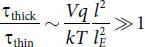
Fig. 3 Diffusion of the photogenerated electrons and holes to the electrodes in a ‘thick’ device. White circles represent defect recombination centers. The figure is aimed to show that interactions with such centers may be likely when charge carriers exercise long-time diffusion movements.
Based on the latter estimate, thin film PV can operate in the opposite limit τ ≪ τ rwhere the role of defect related recombination is on average insignificant. Unfortunately, they have other vulnerabilities related to lateral nonuniformity of their parameters. From a very general point of view, such nonuniformity originates from the lack of transversal self-averaging across too thin structures, which allows significant fluctuations between different spots. Due to device thinness, some sparse spots represent parasitic conductive paths (ohmic or non-ohmic) between opposite electrodes. These paths work as recombination highways degrading PV efficiency. We emphasize that such a nonuniform recombination is qualitatively different from that by point defects in thick PV and call for different mitigating strategies.
Furthermore, having reached the electrodes their respected terminals, electrons and holes undergo fast lateral transport inside the contact metals taking them to the above mentioned recombination channels, through which they disappear. We will see in what follows that the recombination times τ rcof such channels (presented in Fig. 4) form an exponentially broad spectrum decaying towards shorter values. The channels with characteristic recombination times of the order of charge carrier travel times τ dominate because the channels with τ rc≫ τ are inefficient, while those with τ rc≪ τ are too rare. This feature is more quantitatively explained in Sec. XVIfollowing Fig. 104 and subsequent chapters. At this point, we conclude that thin film PV can operate through multidimensional processes where electric currents across and along films are strongly coupled. From the practical perspective, surface treatments that can block the recombination channels appear to be a strategy improving thin film efficiency. That approach has been successful as established on purely empirical grounds before it was theoretically substantiated.
D. Distinctive Features of Thin Film PV
Another distinctive feature of thin film PV is that their forming layers are noncrystalline, but rather polycrystalline (CdTe and CIGS types of PV) or amorphous (a-Si:H based PV). That type of ‘imperfect’ morphology is inevitable with inexpensive fast deposition techniques not giving enough time for satisfactory crystallization. The polycrystalline films consist of tightly packed individual grains, each having more or less perfect crystalline order inside. They are formed during deposition and subsequent treatments where random atomic configurations are ordered within local regions dictating grain sizes. In the course of such crystallization, material pushes away all ‘foreign’ atoms and structural units towards grain boundaries (GB). (Similar to apples in a freezer where water crystallization breaks and pushes away organic tissues.) As a result, GB material is chemically different from that of interior. These chemical differences entail built-in electric fields that will spatially separate electrons and holes between the grain interior and GB (see Fig. 5) creating local electric field and potential variations. One other general consequence of independently forming grains is that having grown enough they compete for space and exert pressure on each other upon physical contact. The resulted compressive stress can translate into electric potential when the material structure is piezo-active, such as with CdS, ZnO and some others, as explained more in detail next ( Sec. XVIII).
Читать дальшеИнтервал:
Закладка:
Похожие книги на «Physics of Thin-Film Photovoltaics»
Представляем Вашему вниманию похожие книги на «Physics of Thin-Film Photovoltaics» списком для выбора. Мы отобрали схожую по названию и смыслу литературу в надежде предоставить читателям больше вариантов отыскать новые, интересные, ещё непрочитанные произведения.


Обсуждение, отзывы о книге «Physics of Thin-Film Photovoltaics» и просто собственные мнения читателей. Оставьте ваши комментарии, напишите, что Вы думаете о произведении, его смысле или главных героях. Укажите что конкретно понравилось, а что нет, и почему Вы так считаете.