Perovskite Materials for Energy and Environmental Applications
Здесь есть возможность читать онлайн «Perovskite Materials for Energy and Environmental Applications» — ознакомительный отрывок электронной книги совершенно бесплатно, а после прочтения отрывка купить полную версию. В некоторых случаях можно слушать аудио, скачать через торрент в формате fb2 и присутствует краткое содержание. Жанр: unrecognised, на английском языке. Описание произведения, (предисловие) а так же отзывы посетителей доступны на портале библиотеки ЛибКат.
- Название:Perovskite Materials for Energy and Environmental Applications
- Автор:
- Жанр:
- Год:неизвестен
- ISBN:нет данных
- Рейтинг книги:5 / 5. Голосов: 1
-
Избранное:Добавить в избранное
- Отзывы:
-
Ваша оценка:
Perovskite Materials for Energy and Environmental Applications: краткое содержание, описание и аннотация
Предлагаем к чтению аннотацию, описание, краткое содержание или предисловие (зависит от того, что написал сам автор книги «Perovskite Materials for Energy and Environmental Applications»). Если вы не нашли необходимую информацию о книге — напишите в комментариях, мы постараемся отыскать её.
The book provides a state-of-the-art summary and discussion about the recent progress in the development and engineering of perovskite solar cells materials along with the future directions it might take.
Audience
Perovskite Materials for Energy and Environmental Applications — читать онлайн ознакомительный отрывок
Ниже представлен текст книги, разбитый по страницам. Система сохранения места последней прочитанной страницы, позволяет с удобством читать онлайн бесплатно книгу «Perovskite Materials for Energy and Environmental Applications», без необходимости каждый раз заново искать на чём Вы остановились. Поставьте закладку, и сможете в любой момент перейти на страницу, на которой закончили чтение.
Интервал:
Закладка:
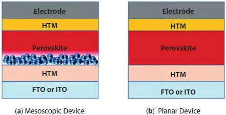
Figure 2.5 Depiction of two main types of PSC [12].
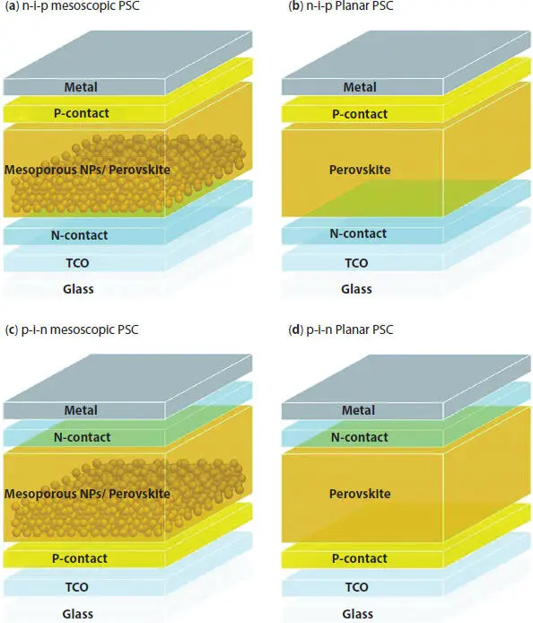
Figure 2.6 Schematic diagram of four types of perovskite solar cell. (a) n-i-p mesoporous structure, (b) p-i-n mesoporous structure, (c) n-i-p planar structure, (d) p-i-n planar structure [13].
The most typical mesoporous framework material is TiO 2. Bi et al. achieved PCE of 20.8%, which contains TiO 2as the mesoporous layer and Spiro-OMeTAD as the electron and hole specified contacts [16]. The limitation of using TiO 2as a mesoporous layer is comparatively low electron mobility [17]. In place of TiO 2, Al 2O 3, and ZnO have also been used as a mesoporous layer [18]. ZnO has two orders of magnitude of electron mobility higher than TiO 2[19]. The recombination rate of charge is significantly slower in TiO 2as compared with Al 2O 3[20]. Also, Zn 2SnO 4, BaSnO 3, and SrTiO 3are tested as mesoporous layers. Zn 2SnO 4-based PSC showed fast electron transport (up to 10 times) and greater charge collection capability as compared with TiO 2-based PSC with the same physical and chemical conditions [21]. BaSnO 3has a large bandgap and relatively higher electron mobility than TiO 2. BaSnO 3was able to achieve 12.3% but has a recombination rate greater than TiO 2[22]. SrTiO 3had achieved 1.01 eV open-circuit voltage, which is 25% higher than TiO 2[23]. The most common hole transport material is Spiro-OMeTAD(2,2′,7,7′-Tetrakis [N,N-di(4-methoxyphenyl)amino]-9,9′-spirobifluorene). An alternative to Spiro-OMeTAD, spiro[fluorene-9,9′-xanthene], achieved the PCE of 19.8% with low fabrication cost [16]. KTM3 showed higher V oc(1.08V) and FF (78.3%) than Spiro-OMeTAD [24]. The commonly used counter electrode materials are Ag, Au, and Pt. For large-scale and continuous production of PSC containing the mesoporous layer of TiO 2, the electrospray deposition method is more viable [25].
2.4.2 Planar Heterostructures
Planar heterostructure is an evolution of the mesoporous structure. The main difference in the planar heterostructure is the absence of the mesoporous layer. The perovskite material is sandwiched between ETM and HTM. Hence, it results in a simpler structure. The planar structure can achieve high PCE even in the absence of a mesoporous layer by carefully controlling the interfaces between layers. There are two interfaces present. First is in between ETM and perovskite and second in between perovskite and HTM. Therefore, electron and hole pairs are separated quickly and efficiently by these two interfaces. The planar structure gives better insight in the understanding of the mechanism of photon absorption and charge separation, which will be useful for better optimization of the PSC. The configuration of planar heterostructure is FTO, ETM, perovskite layer, HTM, electrode layer. FAPbI 3solution-processed planar heterostructure PSC showed PCE of 14.2% with large diffusion length and large tunable bandgap [26]. The planar heterostructure PSC constructed with vapor deposition showed PCE of 15% [27]. J-V hysteresis significantly depends on HTM in planar heterostructures. However, it became negligible when Spiro-OMeTAD was replaced with poly(3,4-ethylene dioxythiophene)-poly(styrene sulfonate) (PEDOT: PSS) or any other inorganic HTM [28]. Moreover, J-V hysteresis also depends on the voltage scan direction, scan rate, and range [29]. In the inverted planar heterostructure (p-i-n), HTM is deposited before ETM. The holes travel themselves in an inverted planar heterostructure [29]. It has been stated that if inverted planar heterostructure PSC is made by mixing methylammonium bromide as an additive in lead acetate and methylammonium iodide solution, maximum PCE of 18.3% is achieved [30].
2.5 Properties
2.5.1 High Optical Absorption
The absorber layer is generally referred to as the heart of the solar cell. The material of this absorber is made of organic inorganic hybrid perovskite. This absorber material has a direct band gap with high absorption coefficient. These properties have permitted to be used as very thin compact absorber materials for gathering light which have thickness in the range of hundreds of nanometers. Whereas the thickness of the film for the traditional solar cell (silicon and germanium) is the range of one micrometer to hundreds of micrometers.
Out of the three generations of solar cell, the first-generation absorber is an indirect bandgap semiconductor material. In this type of semiconductor, the minimum value of conduction band and maximum value of valence band does not lie for the same value of k. Because of this, the momentum of the electron in conduction and valence band is different.
In indirect bandgap semiconductor, transition of photon is horizontal in nature; hence, the momentum of photon is comparatively larger. So a large change of momentum is required for electron-hole pair recombination, hence momentum is not conserved here as k value for both the bands is different. Hence, a large change in momentum is required for recombination of the electron-hole pair as compared with direct bandgap semiconductors. So there is a prohibition for transition of electrons between these two levels and the transition becomes weak because of the participation of lattice vibrations during excitation. Hence, the probability of transition is lower in indirect band gap material than those in direct band gap material. Thus, the thickness of the absorber material of indirect bandgap semiconductor is way more than that of direct band gap semiconductor material for absorbing identical number of photons per unit area [32]. Because of this, for achieving alike efficiency, there is a rise in cost of production of indirect bandgap semiconductor material solar cells as compared with direct band gap semiconductor material solar cells.
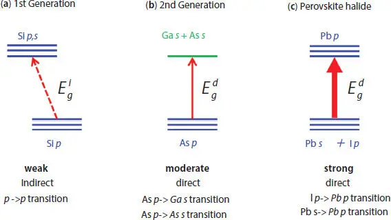
Figure 2.7 Transitions in direct and indirect semiconductor [33].
Second-generation absorber material (GaAs) and perovskite (CH 3NH 3PBI 3) have direct band gap; hence, they have high optical absorption properties compared to silicon. However, their electronic configuration of both the absorbers is not the same as shown in Figure 2.7. The lower part of conduction of gallium arsenide is obtained from the delocalized s orbitals, whereas the lower part of CH 3NH 3PBI 3mainly consists of Pb p bands. The p orbital is less dispersed as compared to s orbitals [33]. Hence, in GaAs, the transition efficiency is moderate. There is a high probability of transition from intra-atomic Pb s to Pb p, because of this, in CH 3NH 3PBI 3, the transition probability between the two bands is almost equivalent to GaAs [33]. Therefore, the optical absorptions are stronger in halide perovskites than GaAs.
2.5.2 High Open-Circuit Voltage
The most distinct property of the PSC technology is their high open circuit voltage, which is the maximum voltage that a solar cell can generate [1]. As from Figure 2.8, we can observe that the best PSC has open circuit voltage greater than 1.1V. The loss-in-potential is around 450 meV, which is quite low. There is energy loss of 250 to 300 meV due to thermodynamic constraints, depending on the bandgap) [34].
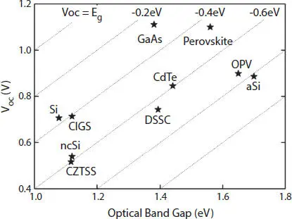
Figure 2.8 Open-circuit voltage (Voc) versus optical band gap (Eg). Reprinted with permission from [1]. Copyright {2013} American Chemical Society.
Читать дальшеИнтервал:
Закладка:
Похожие книги на «Perovskite Materials for Energy and Environmental Applications»
Представляем Вашему вниманию похожие книги на «Perovskite Materials for Energy and Environmental Applications» списком для выбора. Мы отобрали схожую по названию и смыслу литературу в надежде предоставить читателям больше вариантов отыскать новые, интересные, ещё непрочитанные произведения.


Обсуждение, отзывы о книге «Perovskite Materials for Energy and Environmental Applications» и просто собственные мнения читателей. Оставьте ваши комментарии, напишите, что Вы думаете о произведении, его смысле или главных героях. Укажите что конкретно понравилось, а что нет, и почему Вы так считаете.