Christopher Hallinan - Embedded Linux Primer - A Practical, Real-World Approach
Здесь есть возможность читать онлайн «Christopher Hallinan - Embedded Linux Primer - A Practical, Real-World Approach» весь текст электронной книги совершенно бесплатно (целиком полную версию без сокращений). В некоторых случаях можно слушать аудио, скачать через торрент в формате fb2 и присутствует краткое содержание. Год выпуска: 2006, ISBN: 2006, Издательство: Prentice Hall, Жанр: ОС и Сети, на английском языке. Описание произведения, (предисловие) а так же отзывы посетителей доступны на портале библиотеки ЛибКат.

- Название:Embedded Linux Primer: A Practical, Real-World Approach
- Автор:
- Издательство:Prentice Hall
- Жанр:
- Год:2006
- ISBN:978-0-13-167984-9
- Рейтинг книги:4 / 5. Голосов: 1
-
Избранное:Добавить в избранное
- Отзывы:
-
Ваша оценка:
Embedded Linux Primer: A Practical, Real-World Approach: краткое содержание, описание и аннотация
Предлагаем к чтению аннотацию, описание, краткое содержание или предисловие (зависит от того, что написал сам автор книги «Embedded Linux Primer: A Practical, Real-World Approach»). Если вы не нашли необходимую информацию о книге — напишите в комментариях, мы постараемся отыскать её.
This book brings together indispensable knowledge for building efficient, high-value, Linux-based embedded products: information that has never been assembled in one place before. Drawing on years of experience as an embedded Linux consultant and field application engineer, Christopher Hallinan offers solutions for the specific technical issues you're most likely to face, demonstrates how to build an effective embedded Linux environment, and shows how to use it as productively as possible.
Hallinan begins by touring a typical Linux-based embedded system, introducing key concepts and components, and calling attention to differences between Linux and traditional embedded environments. Writing from the embedded developer's viewpoint, he thoroughly addresses issues ranging from kernel building and initialization to bootloaders, device drivers to file systems.
Hallinan thoroughly covers the increasingly popular BusyBox utilities; presents a step-by-step walkthrough of porting Linux to custom boards; and introduces real-time configuration via CONFIG_RT--one of today's most exciting developments in embedded Linux. You'll find especially detailed coverage of using development tools to analyze and debug embedded systems--including the art of kernel debugging.
• Compare leading embedded Linux processors
• Understand the details of the Linux kernel initialization process
• Learn about the special role of bootloaders in embedded Linux systems, with specific emphasis on U-Boot
• Use embedded Linux file systems, including JFFS2--with detailed guidelines for building Flash-resident file system images
• Understand the Memory Technology Devices subsystem for flash (and other) memory devices
• Master gdb, KGDB, and hardware JTAG debugging
• Learn many tips and techniques for debugging within the Linux kernel
• Maximize your productivity in cross-development environments
• Prepare your entire development environment, including TFTP, DHCP, and NFS target servers
• Configure, build, and initialize BusyBox to support your unique requirements
Embedded Linux Primer: A Practical, Real-World Approach — читать онлайн бесплатно полную книгу (весь текст) целиком
Ниже представлен текст книги, разбитый по страницам. Система сохранения места последней прочитанной страницы, позволяет с удобством читать онлайн бесплатно книгу «Embedded Linux Primer: A Practical, Real-World Approach», без необходимости каждый раз заново искать на чём Вы остановились. Поставьте закладку, и сможете в любой момент перейти на страницу, на которой закончили чтение.
Интервал:
Закладка:
At first glance, programming an SDRAM controller can seem like a formidable task. Indeed, numerous Synchronous Dynamic Random Access Memory (DRAM) technologies have been developed. In a never-ending quest for performance and density, many different architectures and modes of operation have been developed.
We examine the AMCC PowerPC 405GP processor for this discussion of SDRAM interface considerations. You might want to have a copy of the user manual to reference while we explore the issues related to SDRAM interfacing. This document is referenced in Section D.4.1, "Suggestions for Additional Reading."
D.1. SDRAM Basics
To understand SDRAM setup, it is necessary to understand the basics of how an SDRAM device operates. Without going into the details of the hardware design, an SDRAM device is organized as a matrix of cells, with a number of address bits dedicated to row addressing and a number dedicated to column addressing. Figure D-1 illustrates this.
Figure D-1. Simplified SDRAM block diagram
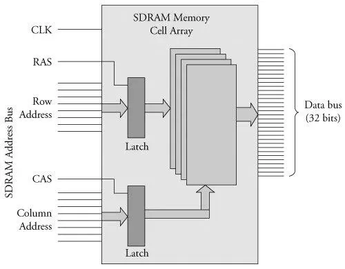
Inside the memory matrix, the circuitry is quite complex. A simplified example of a read operation is as follows: A given memory location is referenced by placing a row address on the row address lines and then placing a column address on the column address lines. After some time has passed, the data stored at the location addressed by the row and column inputs are made available to the processor on the data bus.
The processor outputs a row address on the SDRAM address bus and asserts its Row Address Select (RAS) signal. After a short preprogrammed delay to allow the SDRAM circuitry to capture the row address, the processor outputs a column address and asserts its Column Address Select (CAS) signal. The SDRAM controller translates the actual physical memory address into row and column addresses. Many SDRAM controllers can be configured with the row and column width sizes; the PPC405GP is one of those examples. Later you will see that this must be configured as part of the SDRAM controller setup.
This example is much simplified, but the concepts are the same. A burst read, for example, which reads four memory locations at once, outputs a single RAS and CAS cycle, and the internal SDRAM circuitry automatically increments the column address for the subsequent three locations of the burst read, eliminating the need for the processor to issue four separate CAS cycles. This is but one example of performance optimization. The best way to understand this is to absorb the details of an actual memory chip. An example of a well-written data sheet is included in Section D.4.1, "Suggestions for Additional Reading."
D.1.1. SDRAM Refresh
An SDRAM is composed of a single transistor and a capacitor. The transistor supplies the charge, and the capacitor's job is to retain (store) the value of the individual cell. For reasons beyond the scope of this discussion, the capacitor can hold the value for only a small duration. One of the fundamental concepts of dynamic memory is that the capacitors representing each cell must be periodically recharged to maintain their value. This is referred to as SDRAM refresh.
A refresh cycle is a special memory cycle that neither reads nor writes data to the memory. It simply performs the required refresh cycle. One of the primary responsibilities of an SDRAM controller is to guarantee that refresh cycles are issued in time to meet the chip's requirements.
The chip manufacturers specify minimum refresh intervals, and it is the designer's job to guarantee it. Usually the SDRAM controller can be configured directly to select the refresh interval. The PowerPC 405GP presented here has a register specifically for this purpose. We will see this shortly.
D.2. Clocking
The term synchronous implies that the data read and write cycles of an SDRAM device coincide with the clock signal from the CPU. SDR SDRAM is read and written on each SDRAM clock cycle. DDR SDRAM is read and written twice on each clock cycle, once on the rising edge of the clock and once on the falling edge.
Modern processors have complex clocking subsystems. Many have multiple clock rates that are used for different parts of the system. A typical processor uses a relatively low-frequency crystal-generated clock source for its primary clock signal. A phase locked loop internal to the processor generates the CPU's primary clock (the clock rate we speak of when comparing processor speeds). Because the CPU typically runs much faster than the memory subsystem, the processor generates a submultiple of the main CPU clock to feed to the SDRAM subsystem. You need to configure this clocking ratio for your particular CPU and SDRAM combination.
The processor and memory subsystem clocks must be correctly configured for your SDRAM to work properly. Your processor manual contains a section on clock setup and management, and you must consult this to properly set up your particular board design.
The AMCC 405GP is typical of processors of its feature set. It takes a single crystal-generated clock input source and generates several internal and external clocks required of its subsystems. It generates clocks for the CPU, PCI interface, Onboard Peripheral Bus (OPB), Processor Local Bus (PLB), Memory Clock (MemClk), and several internal clocks for peripherals such as timer and UART blocks. A typical configuration might look like those in Table D-1.
Table D-1. Typical PPC405GP Clock Configuration
| Clock | Rate | Comments |
|---|---|---|
| Crystal reference | 33MHz | Fundamental reference supplied to processor |
| CPU clock | 133MHz | Derived from processor's internal PLL, controlled by hardware pin strapping and register settings. |
| PLB clock | 66MHz | Derived from CPU clock and configured via hardware pin strapping and register settings. Used for internal processor local bus data interchange among its high-speed modules. |
| OPB clock | 66MHz | Derived from PLB clock and configured via register settings. Used for internal connection of peripherals that do not need high-speed connection. |
| PCI clock | 33MHz | Derived from PLB clock and configured via register settings. |
| MemClk | 100MHz | Drives the SDRAM chips directly. Derived from CPU clock and configured via register settings. |
Decisions about clock setup normally must be made at hardware design time. Pin strapping options determine initial clock configurations upon application of power to the processor. Some control over derived clocks is often available by setting divider bits accessible through processor internal registers dedicated to clock and subsystem control. In the example we present here based on the 405GP, final clock configuration is determined by pin strapping and firmware configuration. It is the bootloader's responsibility to set the initial dividers and any other clock options configurable via processor register bits very early after power is applied.
D.3. SDRAM Setup
After the clocks have been configured, the next step is to configure the SDRAM controller. Controllers vary widely from processor to processor, but the end result is always the same: You must provide the correct clocking and timing values to enable and optimize the performance of the SDRAM subsystem.
As with other material in this book, there is no substitute for detailed knowledge of the hardware you are trying to configure. This is especially so for SDRAM. It is beyond the scope of this appendix to explore the design of SDRAM, but some basics must be understood. Many manufacturers' data sheets on SDRAM devices contain helpful technical descriptions. You are urged to familiarize yourself with the content of these data sheets. You don't need a degree in hardware engineering to understand what must be done to properly configure your SDRAM subsystem, but you need to invest in some level of understanding.
Читать дальшеИнтервал:
Закладка:
Похожие книги на «Embedded Linux Primer: A Practical, Real-World Approach»
Представляем Вашему вниманию похожие книги на «Embedded Linux Primer: A Practical, Real-World Approach» списком для выбора. Мы отобрали схожую по названию и смыслу литературу в надежде предоставить читателям больше вариантов отыскать новые, интересные, ещё непрочитанные произведения.


Обсуждение, отзывы о книге «Embedded Linux Primer: A Practical, Real-World Approach» и просто собственные мнения читателей. Оставьте ваши комментарии, напишите, что Вы думаете о произведении, его смысле или главных героях. Укажите что конкретно понравилось, а что нет, и почему Вы так считаете.