John H. Wohlgemuth - Photovoltaic Module Reliability
Здесь есть возможность читать онлайн «John H. Wohlgemuth - Photovoltaic Module Reliability» — ознакомительный отрывок электронной книги совершенно бесплатно, а после прочтения отрывка купить полную версию. В некоторых случаях можно слушать аудио, скачать через торрент в формате fb2 и присутствует краткое содержание. Жанр: unrecognised, на английском языке. Описание произведения, (предисловие) а так же отзывы посетителей доступны на портале библиотеки ЛибКат.
- Название:Photovoltaic Module Reliability
- Автор:
- Жанр:
- Год:неизвестен
- ISBN:нет данных
- Рейтинг книги:5 / 5. Голосов: 1
-
Избранное:Добавить в избранное
- Отзывы:
-
Ваша оценка:
Photovoltaic Module Reliability: краткое содержание, описание и аннотация
Предлагаем к чтению аннотацию, описание, краткое содержание или предисловие (зависит от того, что написал сам автор книги «Photovoltaic Module Reliability»). Если вы не нашли необходимую информацию о книге — напишите в комментариях, мы постараемся отыскать её.
Photovoltaic Module Reliability A comprehensive treatment of current photovoltaic (PV) technology reliability and necessary improvement to become a significant part of the electric utility supply system Well documented with experimental and practical cases throughout, enhancing relevance to both scientific community and industry Timely contribution to the harmonization of methodological aspects of PV reliability evaluation with test procedures implemented to certify PV module quality Written by a leading international authority in PV module reliability
is an excellent book for anyone interested in PV module reliability, including those working directly on PV module and system reliability and preparing to purchase modules for deployment.
Photovoltaic Module Reliability — читать онлайн ознакомительный отрывок
Ниже представлен текст книги, разбитый по страницам. Система сохранения места последней прочитанной страницы, позволяет с удобством читать онлайн бесплатно книгу «Photovoltaic Module Reliability», без необходимости каждый раз заново искать на чём Вы остановились. Поставьте закладку, и сможете в любой момент перейти на страницу, на которой закончили чтение.
Интервал:
Закладка:
3 Amorphous Silicon (a‐Si): Alloys of a‐Si made of thin‐film hydrogenated silicon (a‐Si:H) can be deposited on either glass superstrates or flexible metallic substrates. Because of the low minority carrier lifetimes in doped a‐Si, p‐i‐n (p‐type, intrinsic, n‐type) cell structures are utilized rather than normal p‐n junctions. Even in undoped a‐Si, the minority carrier lifetimes are short and because of the Staebler‐Wronski effect, in which light induces additional electrically active defects, the thickness of individual layers must be minimized. Therefore, to achieve reasonable efficiencies, multi‐junctions are usually utilized. Commercial a‐Si is typically fabricated with a structure similar to the cross‐sectional drawing in Figure 1.2. The maximum reported efficiency for a‐Si modules is about 12% [17], which is less than the efficiencies of commercially available CdTe or CIGs modules. Commercial a‐Si modules have efficiencies in the 5–8% range after light stabilization. Most a‐Si products are used in consumer‐type products (watches, calculators, etc.) not for power production.
Over the years, there have been a number of efforts to use optical concentration to increase the output power that can be obtained from PV devices. Some of these efforts have resulted in laboratory systems with high efficiencies and good performance. However, to date, none have been able to establish a sustainable commercial market. For this reason, reliability of concentrator PV will not be discussed in this book.
1.3 Module Packaging – Purpose and Types
While the solar cells actually produce the electricity, the module package is important for the continued operation of the solar cells. Often the costs associated with the packaging exceed the costs of the cells themselves. Historically, it is usually the package that fails first, ultimately leading to degradation of the cells, conductors, connectors and diodes resulting in failed or degraded modules. The PV module package provides for the following functions:
Mechanical support – holding the cells in place pointing toward the sun.
Dielectric protection – keeping the high voltage away from people and keeping current from flowing out of the array circuit (to ground or in a loop) where it has the potential to cause a fire. Table 1.2 Typical commercial module constructions.Glass Superstrate: Cry‐Si CellsGlass/encapsulant/cry‐Si cells/encapsulant/backsheetGlass/encapsulant/cry‐Si cells/encapsulant/glassGlass Superstrate: Thin Film CellsGlass/thin film cells on front glass/encapsulant/glass with edge sealGlass/thin film cells on front glass/encapsulant/backsheetGlass/encapsulant/thin film cells on back glass/substrateFlexible substratesTransparent frontsheet/encapsulant/thin film cells/flexible substrateTransparent frontsheet/encapsulant/cry‐Si cells/encapsulant/flexible substrate
Protection of the cells, diodes and interconnects from the weather (UV, rain, humidity, hail, etc.)
Coupling of the maximum amount of light energy possible into the solar cells (at all angles at the wavelengths that the cells can utilize).
Cooling of the cells to minimize their temperature increase.
There are really just a few types of module constructions that make up the vast majority of commercial PV modules. Table 1.2provides a list of the types of typical commercial module constructions. A vast majority of PV modules use glass as the front surface because of its excellent optical properties and as we will see in Chapter 2as the main structural support because of the low thermal expansion coefficient of glass.
The first construction for cry‐Si modules (Glass/encapsulant/c‐Si cells/encapsulant/backsheet) has certainly been used on more modules than any other and still remains the most popular in the industry. Figure 1.3ashows a cross‐sectional drawing of a Glass/encapsulant/cry‐Si cells/encapsulant/backsheet module construction. The second construction for c‐Si modules substitutes a second glass layer for the standard backsheet as shown in cross‐section in Figure 1.3b. This type of construction is becoming more popular especially for use in bifacial designs (modules that produce electricity from light that falls on both sides, not just the front). The third construction for c‐Si modules is a flexible design. This is shown in Figure 1.3c. Flexible modules are usually designed as portable power supplies to be carried and deployed when needed. They are not designed for continuous outdoor exposure.
Thin film cells are deposited onto a foreign substrate. These substrates can be glass where the cells are deposited right side up or upside down depending on the technology of the particular thin film material being used. Figures 1.4aand 1.4bshow the cross section of these two types of module constructions. In Figure 1.4a, the thin film is deposited on the backside of the front glass. This is typical of how CdTe and a‐Si modules are fabricated. Figure 1.4ahas been drawn with edge seals as this is typically how CdTe modules are fabricated today. The edge seals are designed to keep moisture from reaching the active cell area for the lifetime of the product (typically warrantied by the manufacturer for 25 years). In Figure 1.4b, the thin film is deposited on the front side of the back glass. This is typical of how CIS and CIGS modules are fabricated. Figure 1.4bhas also been drawn with edge seals, but edge seals are not as prevalent in these types of modules. In this case, the superstrate can also be made of glass though other materials are often used.

Figure 1.3a Cross‐sectional drawing of glass/encapsulant/cry‐Si cells/encapsulant/backsheet module.
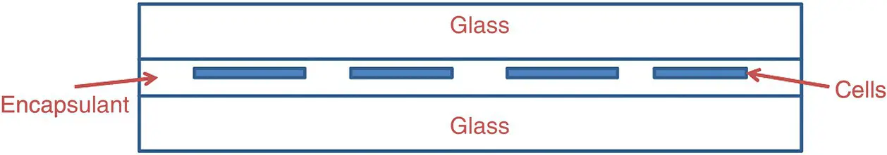
Figure 1.3b Cross‐sectional drawing of glass/encapsulant/cry‐Si cells/encapsulant/glass module.
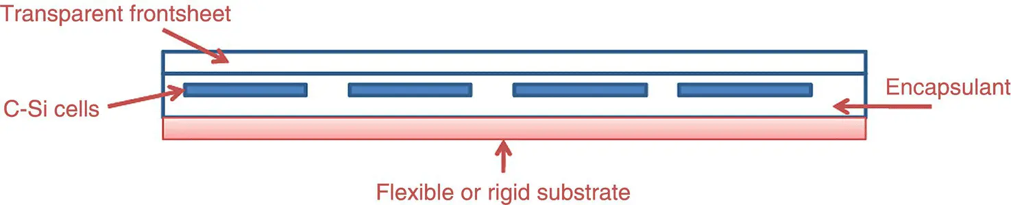
Figure 1.3c Cross‐sectional drawing of flexible cry‐Si module.
In some cases, thin films are deposited in large areas and then cut to cell size afterwards. Basically, creating wafers out of thin films which then have to be electrically connected in series just like cry‐Si cells. Figure 1.4cshows the typical construction used for such thin film modules, although any of the constructions used for cry‐Si wafers could also be used to package these thin film “wafers.” Some CIGS modules have been made with these types of cells. They are particularly of interest for fabrication of large‐area flexible modules.
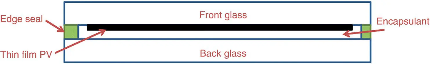
Figure 1.4a Cross‐sectional drawing of front glass/thin film cells/encapsulant/back glass modules.
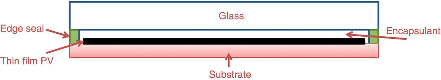
Figure 1.4b Cross‐sectional drawing of front glass/encapsulant/thin film cells/substrate modules.
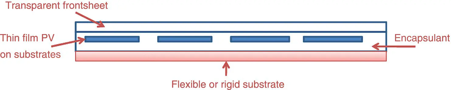
Figure 1.4c Cross‐sectional drawing of module structures for thin film wafer like cells.
Читать дальшеИнтервал:
Закладка:
Похожие книги на «Photovoltaic Module Reliability»
Представляем Вашему вниманию похожие книги на «Photovoltaic Module Reliability» списком для выбора. Мы отобрали схожую по названию и смыслу литературу в надежде предоставить читателям больше вариантов отыскать новые, интересные, ещё непрочитанные произведения.


Обсуждение, отзывы о книге «Photovoltaic Module Reliability» и просто собственные мнения читателей. Оставьте ваши комментарии, напишите, что Вы думаете о произведении, его смысле или главных героях. Укажите что конкретно понравилось, а что нет, и почему Вы так считаете.