John H. Wohlgemuth - Photovoltaic Module Reliability
Здесь есть возможность читать онлайн «John H. Wohlgemuth - Photovoltaic Module Reliability» — ознакомительный отрывок электронной книги совершенно бесплатно, а после прочтения отрывка купить полную версию. В некоторых случаях можно слушать аудио, скачать через торрент в формате fb2 и присутствует краткое содержание. Жанр: unrecognised, на английском языке. Описание произведения, (предисловие) а так же отзывы посетителей доступны на портале библиотеки ЛибКат.
- Название:Photovoltaic Module Reliability
- Автор:
- Жанр:
- Год:неизвестен
- ISBN:нет данных
- Рейтинг книги:5 / 5. Голосов: 1
-
Избранное:Добавить в избранное
- Отзывы:
-
Ваша оценка:
Photovoltaic Module Reliability: краткое содержание, описание и аннотация
Предлагаем к чтению аннотацию, описание, краткое содержание или предисловие (зависит от того, что написал сам автор книги «Photovoltaic Module Reliability»). Если вы не нашли необходимую информацию о книге — напишите в комментариях, мы постараемся отыскать её.
Photovoltaic Module Reliability A comprehensive treatment of current photovoltaic (PV) technology reliability and necessary improvement to become a significant part of the electric utility supply system Well documented with experimental and practical cases throughout, enhancing relevance to both scientific community and industry Timely contribution to the harmonization of methodological aspects of PV reliability evaluation with test procedures implemented to certify PV module quality Written by a leading international authority in PV module reliability
is an excellent book for anyone interested in PV module reliability, including those working directly on PV module and system reliability and preparing to purchase modules for deployment.
Photovoltaic Module Reliability — читать онлайн ознакомительный отрывок
Ниже представлен текст книги, разбитый по страницам. Система сохранения места последней прочитанной страницы, позволяет с удобством читать онлайн бесплатно книгу «Photovoltaic Module Reliability», без необходимости каждый раз заново искать на чём Вы остановились. Поставьте закладку, и сможете в любой момент перейти на страницу, на которой закончили чтение.
Интервал:
Закладка:
In 1994, The Japanese Ministry of Economy, Trade and Industry (METI, formerly called MITI) launched a subsidy program for residential PV systems with an overall goal of installing 4.82 GW of PV by 2010. The program was launched with a subsidy of 50% of the cost of the PV system. The program attracted homeowners not only because of the subsidy, but also because the residential electricity rates in Japan were about 24 Yen/kWh equivalent to about $0.24/kWh at that time, among the highest residential rates in the world. On the other hand, mortgage interest rates in Japan are low (1–2%) and were extendable to cover the costs of residential PV systems. From 1994 until 2003, the Japanese PV market grew steadily by about 30% a year even though the subsidy level was reduced every year. By 2003, the Japanese market was the largest in the world, representing >40% of the world's PV demand.
Germany used a different approach to subsidizing PV systems. Rather than assisting with the initial purchase as was done in Japan, the German program pays a rate or tariff‐based incentive on the electricity actually produced. The PV system owner is paid a specified rate for each kWh produced by the PV system. While such a program had been ongoing in Germany since the late 1990s, a change in the structure of the incentive program that began in 2004, resulted in explosive growth of the German PV market in 2004 and 2005. The feed in tariff rates were established at €45.7 ¢/kWh for ground mounted systems (with a 6.5% annual reduction), at €57.4 ¢/kWh for rooftop residential and at ~€54 ¢/kWh for rooftop commercial (with a 5% annual reduction). In addition to the feed in tariff, preferential loans were made available for PV. This whole program was focused on PV's C02 lowering potential. In Germany, the incentive for PV went from environmental to economic with significant financial returns earned via investment in PV systems. In 2004, the German PV market more than doubled, overtaking Japan as the world's largest PV market. The dramatic market growth was actually constrained in late 2004 and 2005 by lack of module availability.
In the mid‐2000s, China began to realize that PV was going to be an important energy industry and so Chinese companies began manufacturing PV modules. By 2010, an appreciable share of PV modules in the world was being produced in China. By 2015/2016 a majority of all PV modules manufactured in the world were being made in China. The volume has continued to grow since then. The combination of large‐volume production and low costs for labor and infrastructure has led to dramatic decreases in the selling price for PV modules. According to Paula Mints [4] average worldwide module costs have gone from $3.00 to $4.00 per watt in 2007/2008 to less than $0.5 per watt in 2018.
The combination of market need, driven by feed in tariffs and the building of large factories in China led to an explosive growth in the PV industry. With the low cost of modules today, PV is competing successfully with conventional forms of electricity generation. Large (>100 MW) PV systems are being installed around the world with China leading the way both as producer and consumer of PV modules. For a detailed account of the history of how the Photovoltaic Industry began see Peter Varadi's book entitled “Sun Above the Horizon” [10]. For a detailed description of how the PV industry was able to grow so rapidly see Peter's book entitled “Sun Towards High Noon” [11].
1.2 Types of PV Cells
Solar cells are the devices that convert sunlight into electricity. Solar cells are made of semiconductor materials and use a junction to separate the carriers of different charges, that is, to separate the electrons from the holes to create a voltage. There are a number of good articles on how solar cells work including one by the author [12] as well as others in print [13] and on line [14]. This book will not go into great detail about how solar cells work, but will discuss them in terms of how they impact the reliability of PV modules.
A variety of materials have been used commercially to make solar cells. The list below discusses those that have been successfully utilized in terrestrial PV modules and are available commercially today.
Crystalline silicon materials: Crystalline silicon materials were the first utilized for fabrication of solar cells by Bell Laboratories [7]. They were also the first used for space applications and then the first commercialized for remote power terrestrial applications. Crystalline silicon technology has been, and still is, the dominant commercial PV material, with more than 90% of the terrestrial PV market in 2018 [4].
Crystalline Si is a wafer‐based technology. Today, all of the commercial wafers are cut from ingots. There are two different types of crystalline silicon materials, single or mono‐crystalline and multi‐crystalline. They differ in the way the silicon ingots are grown. The single‐crystal ingots are grown by a crystal growth process called Czochralski (CZ), where a single‐crystal seed is dipped into a bath of molten silicon. As the seed is withdrawn, the silicon grows the same orientation as the seed. This is the same process that is used to make the wafers for many semiconductor devices. Single‐crystal ingots are round, but round wafers do not pack very well into rectangular modules so, in most cases, the round wafers are cut into square or pseudo‐square wafers for PV. Multi‐crystalline Si is grown using direction solidification in a crucible or mold. This process was developed specifically for PV in the late 1970s [15]. According to Paula Mints [4], in 2018 multi‐crystalline Si technology accounted for slightly more than 50% of the worldwide shipments of PV modules, while mono‐crystalline Si accounted for approximately 45%.
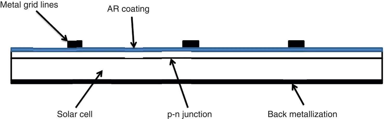
Figure 1.1 Cross‐sectional drawing of screen‐printed cry‐Si solar cell.
For both mono‐ and multi‐crystalline Si, the ingots are cut into wafers using wire saws. The resultant wafers are then processed into cells and the cells incorporated into modules in very similar ways. There are a number of cell processes in use today. Let's take a look at screen‐print technology (one of the simpler methods) since most of the cell components will be similar no matter which cell design is used. Figure 1.1shows a diagram of the important features of a screen‐printed cry‐Si solar cell.
The solar cell is fabricated on the Si wafer. A p‐n junction is grown in the front (sun side) usually by diffusion. Metal grid lines are printed on the front to collect the current generated by the cell. The back side is also metallized. The drawing shows continuous back metallization though a grid can also be used on the back. Finally, because bare silicon is quite reflective, an antireflective coating (AR) is usually applied to the front. For mono‐crystalline Si the front surface is usually textured to increase optical absorption. This is one of the reasons that mono‐crystalline cells are usually a few percent higher in efficiency than multi‐crystalline cells. It is important to remember the different components in the cell when addressing reliability, because it is usually not the Si wafer or the p‐n junction that degrade, but rather the contacts, the interconnections between cells or even the AR coating.
Screen‐printed cry‐Si cells are typically fabricated on 15.6 × 15.6 cm wafers. Over the years, the wafer thickness has been slowly reduced to lower the cost of the Si used in the module. Today, Si wafers are typically less than 200 μm thick, which makes them more susceptible to breakage than the thicker wafers that were used in the earlier days of PV. Today most commercial screen‐printed cells have a conversion efficiency in the range of 15–19% with the multi‐crystalline Si cells at the low end and monocrystalline Si cells at the high end.
Читать дальшеИнтервал:
Закладка:
Похожие книги на «Photovoltaic Module Reliability»
Представляем Вашему вниманию похожие книги на «Photovoltaic Module Reliability» списком для выбора. Мы отобрали схожую по названию и смыслу литературу в надежде предоставить читателям больше вариантов отыскать новые, интересные, ещё непрочитанные произведения.


Обсуждение, отзывы о книге «Photovoltaic Module Reliability» и просто собственные мнения читателей. Оставьте ваши комментарии, напишите, что Вы думаете о произведении, его смысле или главных героях. Укажите что конкретно понравилось, а что нет, и почему Вы так считаете.