John H. Wohlgemuth - Photovoltaic Module Reliability
Здесь есть возможность читать онлайн «John H. Wohlgemuth - Photovoltaic Module Reliability» — ознакомительный отрывок электронной книги совершенно бесплатно, а после прочтения отрывка купить полную версию. В некоторых случаях можно слушать аудио, скачать через торрент в формате fb2 и присутствует краткое содержание. Жанр: unrecognised, на английском языке. Описание произведения, (предисловие) а так же отзывы посетителей доступны на портале библиотеки ЛибКат.
- Название:Photovoltaic Module Reliability
- Автор:
- Жанр:
- Год:неизвестен
- ISBN:нет данных
- Рейтинг книги:5 / 5. Голосов: 1
-
Избранное:Добавить в избранное
- Отзывы:
-
Ваша оценка:
Photovoltaic Module Reliability: краткое содержание, описание и аннотация
Предлагаем к чтению аннотацию, описание, краткое содержание или предисловие (зависит от того, что написал сам автор книги «Photovoltaic Module Reliability»). Если вы не нашли необходимую информацию о книге — напишите в комментариях, мы постараемся отыскать её.
Photovoltaic Module Reliability A comprehensive treatment of current photovoltaic (PV) technology reliability and necessary improvement to become a significant part of the electric utility supply system Well documented with experimental and practical cases throughout, enhancing relevance to both scientific community and industry Timely contribution to the harmonization of methodological aspects of PV reliability evaluation with test procedures implemented to certify PV module quality Written by a leading international authority in PV module reliability
is an excellent book for anyone interested in PV module reliability, including those working directly on PV module and system reliability and preparing to purchase modules for deployment.
Photovoltaic Module Reliability — читать онлайн ознакомительный отрывок
Ниже представлен текст книги, разбитый по страницам. Система сохранения места последней прочитанной страницы, позволяет с удобством читать онлайн бесплатно книгу «Photovoltaic Module Reliability», без необходимости каждый раз заново искать на чём Вы остановились. Поставьте закладку, и сможете в любой момент перейти на страницу, на которой закончили чтение.
Интервал:
Закладка:
A number of commercial cell manufacturers have utilized specialty structures in order to increase cell performance. Several examples are:
SunPower has commercialized cells with all of the contacts on the back of the cell. This cell structure eliminates front surface shadowing and can provide improved collection of the high currents associated with large area cells. This cell structure requires silicon substrates with very high lifetimes and excellent front surface passivation. SunPower offers their commercial cells with conversion efficiency up to 22.7% [16].
The HIT (Heterojunction with intrinsic thin layer) cell uses heterojunctions between a‐Si and crystalline silicon to produce a much higher voltage than the standard p‐n junction. So HIT cells have high efficiency with research cells reported at 25.6% [17] and commercial modules available from Panasonic with reported efficiencies of 19.7% [18].
One of the latest methods for increasing cell efficiency is the use of PERC Technology (Passivated emitter rear cell). PERC cells use the same screen‐printed front surface as standard screen‐print technology, but the rear is modified by replacing the full metal coverage with a passivated dielectric layer with small area back contacts. PERC improves the cells by reducing the back‐surface recombination of carriers and improving the reflection of long wavelength light back into the cells [19]. Solar World has reported PERC cell efficiencies of 22% [20]. There have been a number of forecasts that PERC will gain significant market share in the next few years.
Each solar cell produces a voltage determined by the semiconductor junction. For crystalline Si the typical p‐n junction cell has an open circuit voltage of 0.6–0.7 V and a peak power voltage of around 0.5 V. Therefore, to reach useful voltages a number of cells are connected together in series into a module. Each cell has metal contacts typically copper ribbons attached to the front metal grid and then to the back metallization of the next cell in the string. Ribbons from the front of the cell before it in the string are attached to its back metallization. In this way cell voltages are combined to reach useful levels. Today, most cry‐Si power modules have 60 or 72 cells in series. The next section will talk about the module packaging in more detail.
Thin Films Materials: In the thin‐film approach, the various layers of a PV device are deposited directly onto a substrate or superstrate. The advantages of thin films are the potential ability to:
Dramatically reduce the amount of material utilized. In some cases, the active semiconductor only needs to be a fraction of a micron thick in order to absorb most of the incident sunlight.
Directly integrate into a higher voltage module, thereby eliminating much of the handling and labor necessary to produce cry‐Si modules.
For monolithically integrated thin film modules, the deposition processes and the integration processes are described in Table 1.1and the resultant structure shown in cross section in Figure 1.2. Figure 1.2is not drawn to scale as the thin film layers and the three different scribe lines are exaggerated in size so you can see them. In thin film devices, the semiconductors have considerably higher resistance than cry‐Si so metal grids do not work well. Instead, a Transparent Conductive Oxide (TCO) is often used on the semiconductor surface to provide a conductive path as well as serving as the AR. Because the TCO layers are not as conductive as a metal grid, thin film solar cells are usually long and skinny, so that the collected current only flows a short distance across the cell to the next cell. Monolithically integrated thin film modules often have a large number of skinny cells connected in series, resulting in higher voltage, lower current and reduced series resistance losses.
Thin film layers of materials are more susceptible to corrosion than bulk materials. When thin film layers are deposited directly in contact with glass, they may also be susceptible to ion flow in the glass [21]. This is why many thin film modules are protected in packages that are designed to keep moisture out for the lifetime of the product.
Table 1.1 Process for making monolithically integrated thin film modules.
| Step # | Step Name | Description |
| 1 | Transparent Conductive Oxide TCO | Deposit TCO layer onto the substrate |
| 2 | P1 Scribe | Scribe to remove TCO from selected areas |
| 3 | Semiconductor Deposition | Deposit the semiconductor layers that make the solar cells |
| 4 | P2 Scribe | Scribe to remove the Semiconductors from selected areas |
| 5 | Metallization | Deposit the back metallization |
| 6 | P3 Scribe | Scribe to remove the Metallization from selected areas |
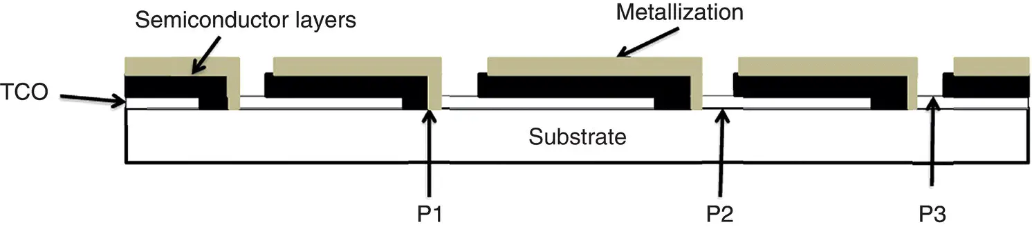
Figure 1.2 Cross‐sectional drawing of monolithically integrated thin film module.
According to Mints [4], thin films only represented about 5% of total worldwide module shipments in 2018, a declining percentage from previous years. The thin‐film PV commercial market includes the following three materials.
1 Cadmium telluride (CdTe): CdTe is a well‐known semiconductor often used in high performance infrared (IR) sensors. CdTe absorbs visible light very strongly, so very thin films (1–2 μm) are sufficient to absorb most of the sunlight. Commercial CdTe modules are typically fabricated on glass with a structure similar to the cross‐sectional drawing in Figure 1.2. First Solar is by far the largest supplier of CdTe modules. First Solar now offers large area, monolithically integrated CdTe modules with efficiencies of up to 18% [22]. CdTe technology is especially attractive because of low‐cost manufacturing. In 2018, First Solar, selling just CdTe modules shipped about 3% of the world's PV modules [4].
2 Copper Indium Diselenide (CIS) and Copper Indium Gallium Diselenide (CIGS): Both CuInSe2 (CIS) and Cu(InGa)Se2 (CIGS) are ideal PV‐absorber materials. The band gap is near the optimum for absorbing the terrestrial spectrum. These materials have strong optical absorption so very thin films (~1 μm) are sufficient to absorb most of the sunlight. Grain boundaries and surfaces in CIS and CIGS are electronically benign, so simple polycrystalline films yield reasonably high efficiency PV devices without complex grain boundary passivation. Typical CIS and CIGS cells use thin CdS layers to form p‐n junctions, molybdenum for ohmic contacts to the CIS or CIGS, and transparent conductors like zinc oxide and indium‐tin oxide for contact to the CdS and to serve as an AR coating. In most cases, CIS and CIGS cells are deposited upside down, meaning that the back metal is deposited first and the cells are deposited from back to front onto the metal. So, CIS and CIGS modules often have the cells deposited onto the back glass of a glass/glass package or onto a metallic substrate that is then diced up to produce individual cells that are packaged like you would wafer‐based cells. While CIS and CIGS are attractive PV materials, it has taken a long time to move from the laboratory to commercialization. Two reasons for this appear to be the difficultly in scaling to larger sizes and larger volumes, related to uniformity of the deposited films, and sensitivity to environmental stresses. Reliability issues relate to the humidity sensitivity of the contacts and TCO necessitating hermetic sealing to achieve long‐term life. Solar Frontier from Japan is the world's largest manufacturer of CIS PV modules offering large area, monolithically integrated CIS modules with conversion efficiencies up to 15% [23]. In 2018, CIS/CIGS made up about 1% of the worldwide shipments of PV modules [4].
Читать дальшеИнтервал:
Закладка:
Похожие книги на «Photovoltaic Module Reliability»
Представляем Вашему вниманию похожие книги на «Photovoltaic Module Reliability» списком для выбора. Мы отобрали схожую по названию и смыслу литературу в надежде предоставить читателям больше вариантов отыскать новые, интересные, ещё непрочитанные произведения.


Обсуждение, отзывы о книге «Photovoltaic Module Reliability» и просто собственные мнения читателей. Оставьте ваши комментарии, напишите, что Вы думаете о произведении, его смысле или главных героях. Укажите что конкретно понравилось, а что нет, и почему Вы так считаете.