Hafiz M. H. Babu - Reversible and DNA Computing
Здесь есть возможность читать онлайн «Hafiz M. H. Babu - Reversible and DNA Computing» — ознакомительный отрывок электронной книги совершенно бесплатно, а после прочтения отрывка купить полную версию. В некоторых случаях можно слушать аудио, скачать через торрент в формате fb2 и присутствует краткое содержание. Жанр: unrecognised, на английском языке. Описание произведения, (предисловие) а так же отзывы посетителей доступны на портале библиотеки ЛибКат.
- Название:Reversible and DNA Computing
- Автор:
- Жанр:
- Год:неизвестен
- ISBN:нет данных
- Рейтинг книги:3 / 5. Голосов: 1
-
Избранное:Добавить в избранное
- Отзывы:
-
Ваша оценка:
Reversible and DNA Computing: краткое содержание, описание и аннотация
Предлагаем к чтению аннотацию, описание, краткое содержание или предисловие (зависит от того, что написал сам автор книги «Reversible and DNA Computing»). Если вы не нашли необходимую информацию о книге — напишите в комментариях, мы постараемся отыскать её.
Reversible and DNA Computing — читать онлайн ознакомительный отрывок
Ниже представлен текст книги, разбитый по страницам. Система сохранения места последней прочитанной страницы, позволяет с удобством читать онлайн бесплатно книгу «Reversible and DNA Computing», без необходимости каждый раз заново искать на чём Вы остановились. Поставьте закладку, и сможете в любой момент перейти на страницу, на которой закончили чтение.
Интервал:
Закладка:
Chapter 11 is also divided into two parts namely reversible random access memory (RAM) and reversible programmable read‐only memory (PROM). In the first part of this chapter, the reversible logic synthesis of RAM is described with a  reversible gate named as FS. In the way of designing a reversible RAM, an
  reversible decoder, reversible D flip‐flop, and write‐enabled master–slave D flip‐flops are also designed. In the second part of this chapter, a reversible PROM design is described. A reversible decoder named ITS and another reversible gate TI are also introduced. In addition, for designing the reversible PROM, an AND‐plane and an Ex‐OR plane are also described. The design of programmable reversible logic gate structures is presented in Chapter 12, which implements ALU and presents its different uses. Finally, a reversible control unit is presented in Chapter 13. Two
  reversible gates, namely HL gate and BJ gate, are introduced to design reversible decoder and JK flip‐flop.
1 Reversible Logic Synthesis
Reversible logic plays a vital role at present time and it has different areas for its applications, namely low‐power CMOS, quantum computing, nanotechnology, cryptography, optical computing, DNA computing, digital signal processing (DSP), quantum‐dot cellular automata (QCA), digital communications, and computer graphics. It is not possible to realize quantum computing without implementation of reversible logic. The main purposes of designing reversible logic circuits are to decrease quantum cost, depth of the circuits, and the number of garbage outputs. This chapter explains the basic reversible logic gates for more complex system, which may have reversible circuits as a primitive component and can execute complicated operations using quantum computers. The reversible circuits form the basic building block of quantum computers, as all quantum operations are reversible. This chapter presents the information related to the primitive reversible gates and helps researchers in designing higher complex computing circuits using reversible gates.
1.1 Reversible Logic
In this section, basic definitions and ideas related to reversible logic are presented. Formal definitions of reversible gate, garbage output, and the popular reversible gates, along with their input–output vectors, are presented here. Illustrative figures and examples are also included in respective discussions.
1.2 Reversible Function
The multiple‐output Boolean function  of n Boolean variables is called reversible if:
1 The number of outputs is equal to the number of inputs.
2 Any output pattern has a unique pre‐image.
In other words, the functions that perform permutations of the set of input vectors are referred to as reversible functions.
1.3 Reversible Logic Gate
Reversible logic has unique mapping between input and output bit pattern. A unit logic entity is represented as a gate. The gates or circuits that do not lose information are called reversible gates or circuits.
Property 1.3.1
A reversible circuit is a circuit in which the number of input and the number of output is equal and there is one‐to‐one mapping between input and output vectors.
Let us consider the gate shown in Figure 1.1. According to the definition, the gate is a reversible gate, because it has k number of inputs and k number of outputs and the gate is known as  reversible gate. Without the NOT gate, classical logic gates are called irreversible, since they cannot determine the input vector states from the output vector states uniquely.
Example 1.1
There can be any number of dimensions for a reversible gate, but lower dimension is always preferable for designing efficient circuits. Popular reversible gates, Feynman gate (FG), Toffoli gate (TG), Peres gate (PG), Fredkin gate (FRG), Feynman double gate (F2G), and new fault‐tolerant gate (NFTG), are shown in Figure 1.2.
1.4 Garbage Outputs
The output (outputs) of a reversible gate that is (are) not used as input to other gate or the output (outputs) that is (are) not treated as a primary output is (are) called garbage output (outputs). The unutilized outputs from a gate are called garbage outputs. A heavy price is paid for every garbage output. So, for any circuit design, the fewer the garbage outputs, the better.
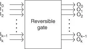
Figure 1.1A  reversible gate.
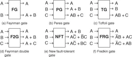
Figure 1.2Popular reversible gates.

Figure 1.3Reversible Feynman gate.
Example 1.2
When a Feynman gate (FG) is used for Ex‐OR (exclusive‐OR,  ) operation of two inputs, an extra output is generated at the output part of the FG in addition to the Ex‐OR output. This additional output is known as garbage output. In Figure 1.3, the garbage output of a gate is shown. Here, A is the garbage output.
1.5 Constant Inputs
Constant inputs are the inputs of a reversible gate (or circuit) that are either set to 0 or 1.
Example 1.3
If the complement of the input A from Figure 1.3is needed, then B is set to 1 and  .
.
1.6 Quantum Cost
The quantum cost of a circuit is the total number of 2  2 quantum primitives that are used to realize corresponding quantum circuit. Basically, the quantum primitives are matrix operations, which are applied on qubits state.
Example 1.4
The quantum realization of reversible Fredkin (FRG) gate is shown in Figure 1.4. Each quantum Ex‐OR gate and quantum  or
or  gate requires 1 (one) quantum cost. The reversible FRG gate has four quantum Ex‐OR gates, two quantum V gates, and one quantum
  gate. So, the quantum cost of reversible FRG gate seems 7 (seven). But, we know if a quantum Ex‐OR gate and a quantum
  or
or  gate exist angularly (denoted by angular box), then the quantum cost is treated as 1. From the figure, we see that there exists two angular boxes, and each angular box is treated as 1 quantum cost. As a result, the total quantum cost of reversible FRG gate is 5 (five).
Интервал:
Закладка:
Похожие книги на «Reversible and DNA Computing»
Представляем Вашему вниманию похожие книги на «Reversible and DNA Computing» списком для выбора. Мы отобрали схожую по названию и смыслу литературу в надежде предоставить читателям больше вариантов отыскать новые, интересные, ещё непрочитанные произведения.


Обсуждение, отзывы о книге «Reversible and DNA Computing» и просто собственные мнения читателей. Оставьте ваши комментарии, напишите, что Вы думаете о произведении, его смысле или главных героях. Укажите что конкретно понравилось, а что нет, и почему Вы так считаете.