Tim Bruton - Photovoltaics from Milliwatts to Gigawatts
Здесь есть возможность читать онлайн «Tim Bruton - Photovoltaics from Milliwatts to Gigawatts» — ознакомительный отрывок электронной книги совершенно бесплатно, а после прочтения отрывка купить полную версию. В некоторых случаях можно слушать аудио, скачать через торрент в формате fb2 и присутствует краткое содержание. Жанр: unrecognised, на английском языке. Описание произведения, (предисловие) а так же отзывы посетителей доступны на портале библиотеки ЛибКат.
- Название:Photovoltaics from Milliwatts to Gigawatts
- Автор:
- Жанр:
- Год:неизвестен
- ISBN:нет данных
- Рейтинг книги:4 / 5. Голосов: 1
-
Избранное:Добавить в избранное
- Отзывы:
-
Ваша оценка:
Photovoltaics from Milliwatts to Gigawatts: краткое содержание, описание и аннотация
Предлагаем к чтению аннотацию, описание, краткое содержание или предисловие (зависит от того, что написал сам автор книги «Photovoltaics from Milliwatts to Gigawatts»). Если вы не нашли необходимую информацию о книге — напишите в комментариях, мы постараемся отыскать её.
Photovoltaics from Milliwatts to Gigawatts: Understanding Market and Technology Drivers toward Terawatts Divided into 9 chapters, the book includes the following topics: Early History; The 1973 Oil crisis and the drive for alternative energies; The emergence in the 1980’s of the off grid PV market, the significant small scale PV consumer market and the establishment of a manufacturing industry; Advantages of silicon for solar cells; The evolution of PV installations; The history of the incentive programme for PV; Difficulties of alternative technologies in challenging silicon dominance; Current status of the silicon manufacturing technology and The future.
Key features:
An authoritative first-hand account of an emerging technology from laboratory to global significance for electricity generation by an industry expert. Provides a framework for policy makers on future trends in the PV industry. Examines the lessons learnt from the interaction of research laboratories, major industry and government. Signposts the route to future high efficiency silicon solar cells giving new researchers a background for further development. Highlights the critical success factors for the emerging alternative manufacturing technologies. An essential PV guide aimed at researchers and students in electrical engineering and physical sciences through the rapid evolution of PV technology to commercial viability and the challenges ahead for increased performance, efficiency and global deployment.
Photovoltaics from Milliwatts to Gigawatts — читать онлайн ознакомительный отрывок
Ниже представлен текст книги, разбитый по страницам. Система сохранения места последней прочитанной страницы, позволяет с удобством читать онлайн бесплатно книгу «Photovoltaics from Milliwatts to Gigawatts», без необходимости каждый раз заново искать на чём Вы остановились. Поставьте закладку, и сможете в любой момент перейти на страницу, на которой закончили чтение.
Интервал:
Закладка:
GaAs has a history almost as long as that of silicon. One of the first GaAs solar cells was made at RCA Laboratories in 1956, with an efficiency of 6% on very small‐area solar cells [66]. From that point on, significant progress was made, driven by the expectation of higher efficiency and enhanced radiation hardness. By 1981, the 20%‐efficiency barrier had been breached, with an n+/p/p+ GaAs structure on both germanium and GaAs substrates [67]. Early GaAs cells were made by liquid‐phase epitaxy, which had limits in terms of the alloys that could be produced, while the 1981 work was performed using vapour‐phase epitaxy. By the late 1990s, however, metal organic chemical vapour deposition (MOCVD) had become a well‐established technique for producing a wide range of III–V compounds [64]. In 1990, cells of over 25% efficiency were demonstrated using MOCVD for the epitaxial layers – in some cases, as thin as 0.1 μm [68]. The best cell had an efficiency of 25.7% under the AM1.5 Global spectrum; its structure is illustrated in Figure 1.13. The improved efficiency was derived in part from the use of a GaInP 2window at front and rear, such that the active carrier collection region was separated from the high recombination surfaces at the front and rear of the active GaAs cell.
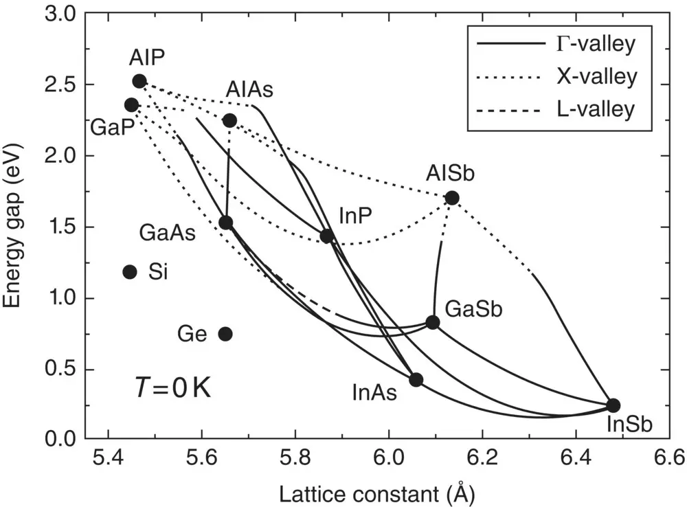
Figure 1.12 Bandgap and lattice constant for the important III–V alloys [62]
(Courtesy Royal Society of Chemistry) Source: H. Cotal et al: Energy and Environmental Science 2 (2009) 174‐192
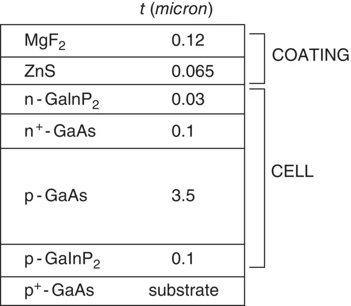
Figure 1.13 Structure of a 25.7% GaAs solar cell under the AM1.5 Global spectrum [68]
(Courtesy IEEE) Source: S.R. Kurtz, J.M. Olsen and A. Kibbler: Proc 21st IEEE PVSC (1990) 138‐140
GaInP 2was used in preference to the GaAlAs 2previously employed, as this was prone to degradation by the inclusion of oxygen. The work highlighted that the electronic quality of the individual layers was as important as the overall device structure in achieving very high efficiencies. Development of single‐junction GaAs has been relatively slow, as more research has gone into the higher‐efficiency potential triple‐junction cells. In 2008, the record efficiency was 26.1% [69]; in 2018, Alta Devices reported a new record for single‐junction GaAs cells of 28.9% [70], in the form of an ultrathin cell. This was intended not for space applications but for terrestrial ones, where very high efficiency is important (e.g. the Internet of Things, unmanned aircraft).
1.4.2 Multijunction Solar Cells for Space
The first successful GaAs heterojunction solar cell was demonstrated in 1970 for a GaAlAs/GaAs structure [71]. Good progress was made, and by 1981 an AM0 efficiency of 15% was posted for a GaAs/GaAlAs tandem [72]. At the same time, it was observed that germanium could also be used as a substrate, as it is also lattice matched to GaAs, as shown in Figure 1.12[67]. At this point in time, liquid‐phase epitaxy was the preferred method for making the tandem cells. Lattice matching is important as if a significant mismatch occurs, the stress at the interface between two semiconductors creates threading dislocations which spread through the epitaxial layers and act as recombination centres. These have a great impact in reducing the solar cell efficiency. Removing the lattice‐matching constraint means a wider range of III–V compounds can be used, with greater potential for high efficiency. In this case, alternating layers with different lattice parameters of stress and compression can prevent the generation of threading dislocations. These are known as metamorphic cells [64]. In general, space cells have been lattice matched, but metamorphic cells have been developed for concentrator applications. A particular challenge with the use of tandem cells is that there is a p/n junction between the top cell and the bottom one, which is rectifying for the direction of current flow. To overcome this, a heavily doped ‘tunnel junction’ is used, in which carriers can travel through the rectifying junction, as illustrated in Figure 1.14[73]. The requirements of the tunnel junction are that it be a wide‐bandgap semiconductor for good transparency and that it be heavily doped in order for tunnelling to occur. This makes for an added complexity and cost for tandem cells.
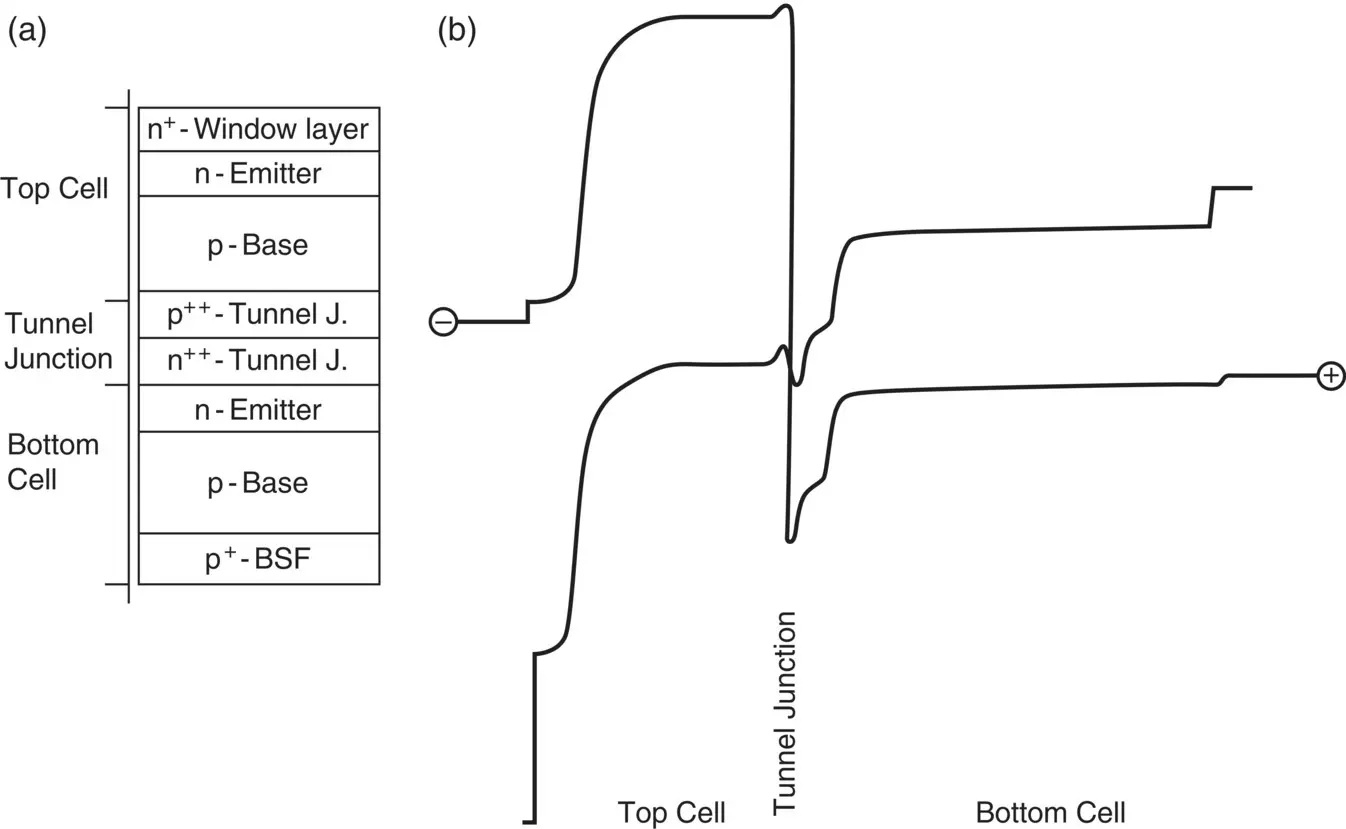
Figure 1.14 (a) Structure of a tandem cell, showing the tunnel junction.
Source: N.J. Ekins‐Daukes: in “Solar Cell Materials‐Developing Technologies” ed G J Conibeer and A Willoughby. Pub J Wiley (2014) 113‐143
(b) Associated band diagram, highlighting the tunnelling effect [73]
(Courtesy Wiley) Source: N.J. Ekins‐Daukes: in “Solar Cell Materials‐Developing Technologies” ed G J Conibeer and A Willoughby. Pub J Wiley (2014) 113‐143
As already described, the availability of MOCVD deposition systems greatly assisted the development of III–V epitaxial growth. By 1995, the practical limit for a GaInP 2/GaAs tandem cell of 30% was reached [74]. At the same time, efforts were underway to fabricate III–V cells for use in space. Germanium was preferred to GaAs as the substrate, as it was physically much more robust. Initially, it was only used as an inactive substrate, but its low bandgap at 0.7 eV made it ideal for use as the bottom cell in triple‐junction tandem. Initial production of single‐junction GaAs/Ge cells was reported in 1990, with AM0 spectrum cells achieving 18% efficiency for a 4 × 2 cm cell [75].
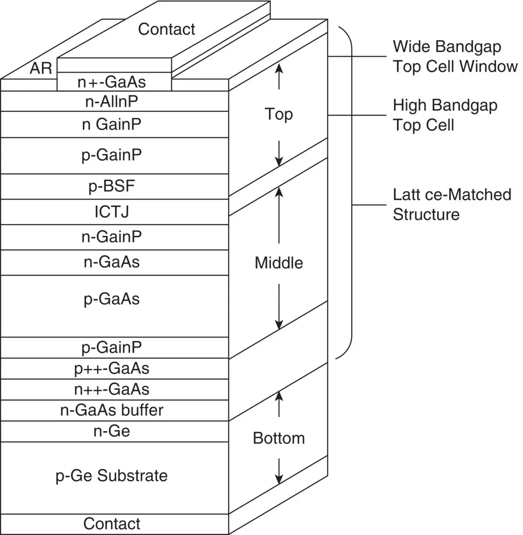
Figure 1.15 Structure of a very high‐efficiency triple‐junction tandem III–V solar cell [78]
(Courtesy Wiley) Source: H. Yoon et al: Progress in Photovoltaics‐Research and Applications. 13 (2005) 133–139
By 1996, double cells were being made with GaAs/Ge, and a best cell with an efficiency of 23.8% was reported [76]. At the same time, results were being published for triple‐junction GaInP 2/GaAs/Ge cells with an efficiency of 25.7% (4 cm 2) [77]. The first commercial satellite with dual‐junction cells was launched in 1998, with initial cell efficiencies of 22%. By 2005, triple‐junction cells with an initial efficiency of 28.0% (AM0 spectrum) were being manufactured [78]. The structure of a triple‐junction solar cell is depicted in Figure 1.15, which shows the complexity of the device structure. The current best efficiencies being manufactured for use in space belong to triple‐junction cells, at 32% at beginning of life and a projected 30% after 15 years’ space exposure [79]. Figure 1.16shows the assembly of current solar panels for use in space.
1.5 Summary
This chapter has described how photovoltaics evolved from some very simple experiments in the early nineteenth century to become a key enabling technology for the reliable functioning of satellite systems. Much of the current digital age relies heavily on the ability of satellites to communicate data; without them, modern society would not function. The development of solar cells for space use was the foundation stone for the large‐scale terrestrial industry that exists today. Subsequent chapters in this book describe how this technology migration occurred and how it continues to develop toward large‐scale deployment at the terawatt scale.
Читать дальшеИнтервал:
Закладка:
Похожие книги на «Photovoltaics from Milliwatts to Gigawatts»
Представляем Вашему вниманию похожие книги на «Photovoltaics from Milliwatts to Gigawatts» списком для выбора. Мы отобрали схожую по названию и смыслу литературу в надежде предоставить читателям больше вариантов отыскать новые, интересные, ещё непрочитанные произведения.


Обсуждение, отзывы о книге «Photovoltaics from Milliwatts to Gigawatts» и просто собственные мнения читателей. Оставьте ваши комментарии, напишите, что Вы думаете о произведении, его смысле или главных героях. Укажите что конкретно понравилось, а что нет, и почему Вы так считаете.