Tim Bruton - Photovoltaics from Milliwatts to Gigawatts
Здесь есть возможность читать онлайн «Tim Bruton - Photovoltaics from Milliwatts to Gigawatts» — ознакомительный отрывок электронной книги совершенно бесплатно, а после прочтения отрывка купить полную версию. В некоторых случаях можно слушать аудио, скачать через торрент в формате fb2 и присутствует краткое содержание. Жанр: unrecognised, на английском языке. Описание произведения, (предисловие) а так же отзывы посетителей доступны на портале библиотеки ЛибКат.
- Название:Photovoltaics from Milliwatts to Gigawatts
- Автор:
- Жанр:
- Год:неизвестен
- ISBN:нет данных
- Рейтинг книги:4 / 5. Голосов: 1
-
Избранное:Добавить в избранное
- Отзывы:
-
Ваша оценка:
Photovoltaics from Milliwatts to Gigawatts: краткое содержание, описание и аннотация
Предлагаем к чтению аннотацию, описание, краткое содержание или предисловие (зависит от того, что написал сам автор книги «Photovoltaics from Milliwatts to Gigawatts»). Если вы не нашли необходимую информацию о книге — напишите в комментариях, мы постараемся отыскать её.
Photovoltaics from Milliwatts to Gigawatts: Understanding Market and Technology Drivers toward Terawatts Divided into 9 chapters, the book includes the following topics: Early History; The 1973 Oil crisis and the drive for alternative energies; The emergence in the 1980’s of the off grid PV market, the significant small scale PV consumer market and the establishment of a manufacturing industry; Advantages of silicon for solar cells; The evolution of PV installations; The history of the incentive programme for PV; Difficulties of alternative technologies in challenging silicon dominance; Current status of the silicon manufacturing technology and The future.
Key features:
An authoritative first-hand account of an emerging technology from laboratory to global significance for electricity generation by an industry expert. Provides a framework for policy makers on future trends in the PV industry. Examines the lessons learnt from the interaction of research laboratories, major industry and government. Signposts the route to future high efficiency silicon solar cells giving new researchers a background for further development. Highlights the critical success factors for the emerging alternative manufacturing technologies. An essential PV guide aimed at researchers and students in electrical engineering and physical sciences through the rapid evolution of PV technology to commercial viability and the challenges ahead for increased performance, efficiency and global deployment.
Photovoltaics from Milliwatts to Gigawatts — читать онлайн ознакомительный отрывок
Ниже представлен текст книги, разбитый по страницам. Система сохранения места последней прочитанной страницы, позволяет с удобством читать онлайн бесплатно книгу «Photovoltaics from Milliwatts to Gigawatts», без необходимости каждый раз заново искать на чём Вы остановились. Поставьте закладку, и сможете в любой момент перейти на страницу, на которой закончили чтение.
Интервал:
Закладка:
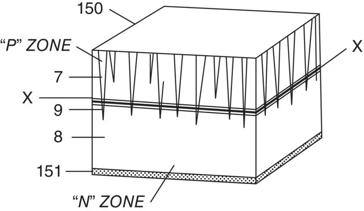
Figure 1.3 Ohl’s patented solar cell structure [20]
Source: R.S. Ohl: US Patent Application filed 27th May 1941
Russel Ohl, a Bell Labs scientist interested in exploring the crystallisation of silicon, is recognised as the discoverer of the p/n junction in this material, in 1941 [19]. In directionally solidifying 99.85% pure silicon, Ohl noted a change in the structure of the solidified ingot, with the upper portion becoming columnar and the lower portion showing no structure; a striated region appeared between the two, forming a barrier to conduction. The upper zone was p type while the lower zone was n type [20]. This can be easily understood as a result of the segregation of dopants during the crystallisation process. While measuring the resistance of rods containing the barrier, Ohl noted a sensitivity to light, which he termed a ‘photo electromotive force’. He proceeded to patent this as a solar cell, although its efficiency was similar to that of the selenium cells, at about 1% [20]. Figure 1.3shows Ohl’s silicon structure, the n type region being fine‐grained crystallites and the cell contacts plated rhodium. The low efficiency is not surprising given the relatively impure starting material, its multicrystalline nature, and the fact that the n type region was 0.5 mm thick. The relatively low efficiency meant little further work was done until a new approach at Bell Labs.
Success came in the 1950s. The first transistor had been demonstrated at Bell in 1948 using germanium, and had entered commercial production in 1951 [21]. However, germanium had some disadvantages in its fragility and stability, and silicon offered a better option – although a working silicon transistor was not demonstrated until 1954. Two scientists working on this were Calvin S. Fuller and Gerald L. Pearson. Fuller was an expert in doping silicon, while Pearson was an experimentalist. There were three iterations before a good working solar cell was demonstrated [22]. Initially, while not looking for a solar cell, Fuller produced a p type gallium‐doped silicon sample, which Pearson dipped into a lithium bath to form a shallow n type region. When Pearson exposed the sample to light, he found to his surprise that a current was generated. At the same time, in a different department, another scientist, Daryl M. Chapin, was looking for a power source for telecommunications repeaters in hot humid locations where conventional dry cell batteries rapidly failed. Chapin concluded that solar cells were a good option, but his experiments with commercial selenium cells of low efficiency were disappointing. He and Pearson knew each other, and Pearson offered Chapin his lithium‐doped ‘solar cell’. Chapin tested it and found it 2.3% efficient – an enormous improvement on selenium, justifying further investigations into silicon’s potential. The next step was to replace the lithium with phosphorus. A small amount of phosphorus was evaporated on to the p type silicon to make a shallow n type region. Initial results weren’t particularly good, but then Chapin applied a thin plastic layer to act as an antireflection coating (ARC) on the otherwise highly reflecting silicon surface. This gave the encouraging result of around 4% cell efficiency, which was good progress toward Chapin’s target of 5.7% for a viable power source. However, further progress was slow, and forming a good electrical contact proved to be an ongoing problem. A spur to further activity came from Bell’s competitor, RCA, which was developing an ‘atomic battery’ using a strontium 90 source to irradiate a silicon solar cell, although efficiencies were poor. The breakthrough came when Fuller, who had been experimenting with boron to give a p type silicon emitter which offered a new configuration, demonstrated that heating an n type silicon wafer for 5.5 hours at 1000 °C in a boron trichloride atmosphere under reduced pressure could produce a 0.25 μm‐deep diffusion with a resistivity of .001 Ω/cm [23]. This equated to 40 Ω per square sheet resistance emitter, which is a typical figure for later commercial silicon solar cells. Arsenic was used to dope the silicon base n type to 0.1 Ω/cm, and this was then cut into long narrow strips in accordance with the best previous cell results. The emitter was formed using the new boron diffusion process, with the emitter itself wrapping around the cell as shown in Figure 1.4. It was then partially removed on the rear to expose the n type base. Contacts were made by electroplating rhodium to the exposed base and emitter [24]; the relative ease in forming these contacts represented a significant advance. A polystyrene layer with refractive index 1.6 was used as the ARC. The solar cell efficiency was approximately 6% [25]. Chapin had proposed a theoretical limit of 22% efficiency for silicon, but had stated that practical limitations would result in its being lower in the real world. The spectral response of the cell is shown in Figure 1.5. It was proposed that 10 cells connected in series would be needed to provide the 1 W of power required to charge the batteries at a repeater station in a rural carrier telephone system [24].
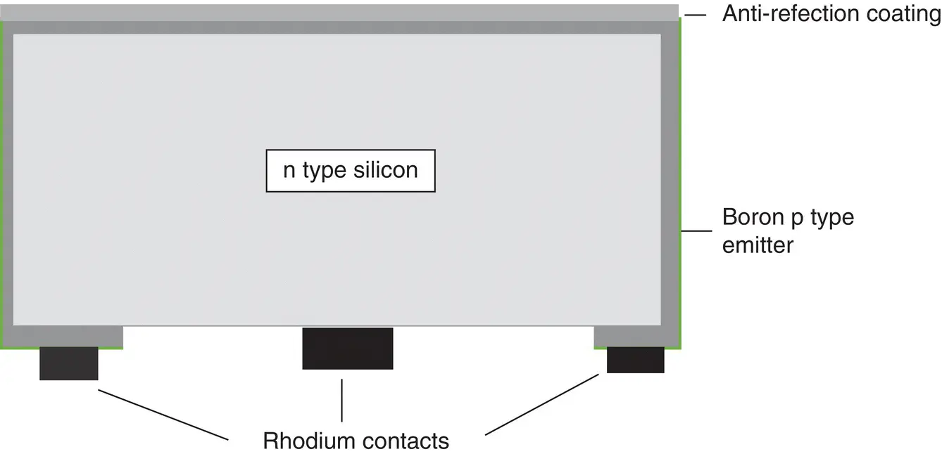
Figure 1.4 Schematic of the first successful silicon solar cell
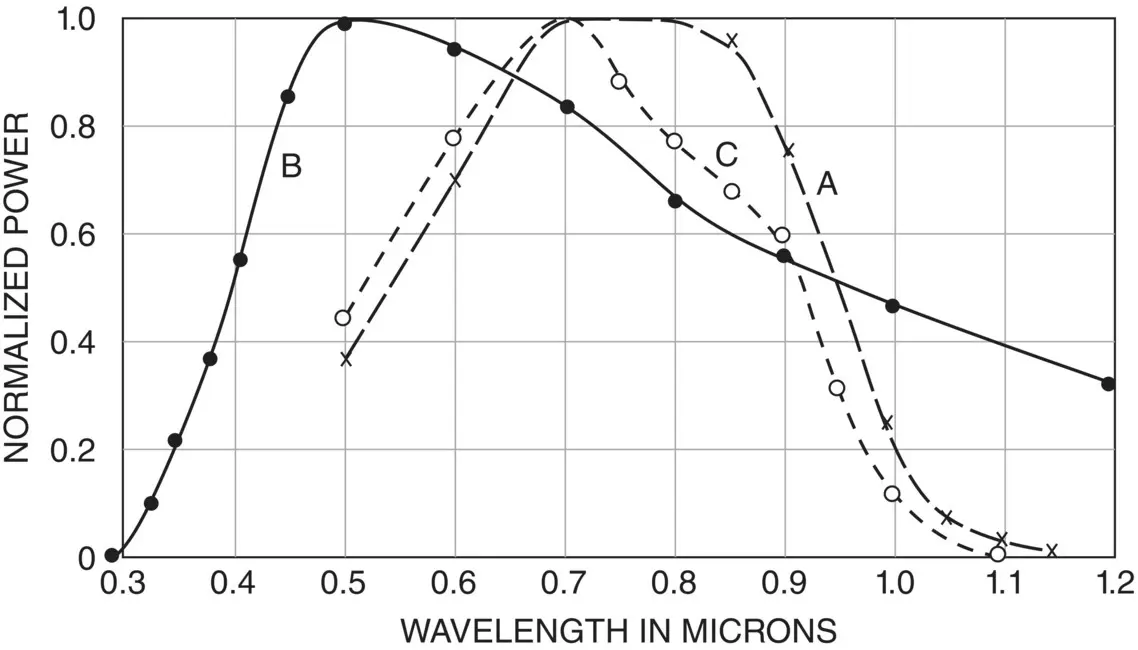
Figure 1.5 (A) Normalised spectral response of a p on n silicon solar cell. (B) Solar spectrum. (C) Relative integrated response [23]
Source: C.S. Fuller: US Patent 3015590, 2nd Jan. 1962 (filed 5th March 1954)
The 6% efficiency result met Chapin’s original target and gave the impetus for further improvement. By November 1954, an 8%‐efficiency cell had been produced with the same wraparound structure [26], and by May 1955, 11% efficiency was demonstrated [27]. It is interesting to note that this structure – an n type wafer with all of the contact metallisation on the rear – has a resonance with the current world‐record silicon solar cell (26.7% efficiency), based on an n type wafer with rear contacts, but with amorphous silicon providing the p side of the junction [28]. In their 1954 patent filing, the inventors stated that ‘Sunlight is the most common, most accessible, and most economical form of energy on the Earth’s surface’ [24]. This group at Bell Labs opened the door for practical exploitation of this rich energy source, although it was a further 20 years before its true potential began to be fully exploited.
1.2.3 Hiatus
While the Bell discovery was heralded as a great breakthrough, with the New York Times stating it ‘may mark the beginning of a new era, leading eventually to the realisation of one of mankind’s most cherished dreams – the harnessing of the almost limitless energy of the sun for the uses of civilisation’ [29] and the US News & World Report claiming ‘the (silicon) strips may provide more power than all the world’s coal, oil and uranium’ [30], the reality in 1954 was somewhat different. The cost of the high‐purity silicon needed to make viable solar cells was very high at $845/kg, resulting in an estimated cost of electricity of $144/kWh, compared to $23.7/kWh for dry cell batteries and less than $0.02/kWh for retail grid electricity [31]. Despite this disadvantage, Bell’s manufacturing subsidiary, Western Electric, took up commercialisation. One of the first applications was powering a remote telephone line in rural Georgia (USA). However, the introduction of silicon transistors for voice amplification with a very low power requirement made the application redundant and activity at Bell largely declined [31]. Western Electric licensed other companies to manufacture the silicon solar cells, one of which, National Fabricated Products, went as far as to assemble a range of demonstration products. But no market was forthcoming and National Fabricated Products was taken over by Hoffman Electronics in 1956. Hoffman provided prototypes for both the US Coast Guard and the US Forest Service, but no business resulted. The initial enthusiasm cooled to the extent that in 1957 it was reported that ‘Viewed in the light of the world’s power needs, these gadgets are toys’ [32].
Читать дальшеИнтервал:
Закладка:
Похожие книги на «Photovoltaics from Milliwatts to Gigawatts»
Представляем Вашему вниманию похожие книги на «Photovoltaics from Milliwatts to Gigawatts» списком для выбора. Мы отобрали схожую по названию и смыслу литературу в надежде предоставить читателям больше вариантов отыскать новые, интересные, ещё непрочитанные произведения.


Обсуждение, отзывы о книге «Photovoltaics from Milliwatts to Gigawatts» и просто собственные мнения читателей. Оставьте ваши комментарии, напишите, что Вы думаете о произведении, его смысле или главных героях. Укажите что конкретно понравилось, а что нет, и почему Вы так считаете.