Tim Bruton - Photovoltaics from Milliwatts to Gigawatts
Здесь есть возможность читать онлайн «Tim Bruton - Photovoltaics from Milliwatts to Gigawatts» — ознакомительный отрывок электронной книги совершенно бесплатно, а после прочтения отрывка купить полную версию. В некоторых случаях можно слушать аудио, скачать через торрент в формате fb2 и присутствует краткое содержание. Жанр: unrecognised, на английском языке. Описание произведения, (предисловие) а так же отзывы посетителей доступны на портале библиотеки ЛибКат.
- Название:Photovoltaics from Milliwatts to Gigawatts
- Автор:
- Жанр:
- Год:неизвестен
- ISBN:нет данных
- Рейтинг книги:4 / 5. Голосов: 1
-
Избранное:Добавить в избранное
- Отзывы:
-
Ваша оценка:
Photovoltaics from Milliwatts to Gigawatts: краткое содержание, описание и аннотация
Предлагаем к чтению аннотацию, описание, краткое содержание или предисловие (зависит от того, что написал сам автор книги «Photovoltaics from Milliwatts to Gigawatts»). Если вы не нашли необходимую информацию о книге — напишите в комментариях, мы постараемся отыскать её.
Photovoltaics from Milliwatts to Gigawatts: Understanding Market and Technology Drivers toward Terawatts Divided into 9 chapters, the book includes the following topics: Early History; The 1973 Oil crisis and the drive for alternative energies; The emergence in the 1980’s of the off grid PV market, the significant small scale PV consumer market and the establishment of a manufacturing industry; Advantages of silicon for solar cells; The evolution of PV installations; The history of the incentive programme for PV; Difficulties of alternative technologies in challenging silicon dominance; Current status of the silicon manufacturing technology and The future.
Key features:
An authoritative first-hand account of an emerging technology from laboratory to global significance for electricity generation by an industry expert. Provides a framework for policy makers on future trends in the PV industry. Examines the lessons learnt from the interaction of research laboratories, major industry and government. Signposts the route to future high efficiency silicon solar cells giving new researchers a background for further development. Highlights the critical success factors for the emerging alternative manufacturing technologies. An essential PV guide aimed at researchers and students in electrical engineering and physical sciences through the rapid evolution of PV technology to commercial viability and the challenges ahead for increased performance, efficiency and global deployment.
Photovoltaics from Milliwatts to Gigawatts — читать онлайн ознакомительный отрывок
Ниже представлен текст книги, разбитый по страницам. Система сохранения места последней прочитанной страницы, позволяет с удобством читать онлайн бесплатно книгу «Photovoltaics from Milliwatts to Gigawatts», без необходимости каждый раз заново искать на чём Вы остановились. Поставьте закладку, и сможете в любой момент перейти на страницу, на которой закончили чтение.
Интервал:
Закладка:
Another approach to increasing solar cell efficiency involved using higher‐resistivity wafers, as these had longer minority carrier diffusion lengths, giving higher short‐circuit currents. However, this came at the cost of a lower Voc, so that there was an overall loss in efficiency [53]. It was also desirable to decrease the wafer thickness in order to improve the electrical yield per unit weight – an important consideration for satellites. It was shown experimentally that Voc above 580 mV could be obtained by a ‘gettering process’ [54]. Further experiments showed that firing an aluminium rear contact produced good results and that a thickness reduction to 200 μm was possible without loss of efficiency and with good radiation hardness [54]. The aluminium rear surface could also act as back surface reflector of light, contributing to improved current generation. The cells produced were termed back surface field (BSF) cells, and at the standard thickness of 300 μm they increased the solar cell efficiency from 9.3 to 11.6%. The mechanism for efficiency improvement was a combination of the p+ doping at the rear creating an internal electric field that repulsed the minority carrier electrons and a gettering action removing impurities from the silicon introduced in processing to give a high minority carrier lifetime. In later years, the BSF approach represented a useful enhancement in terrestrial solar cells.
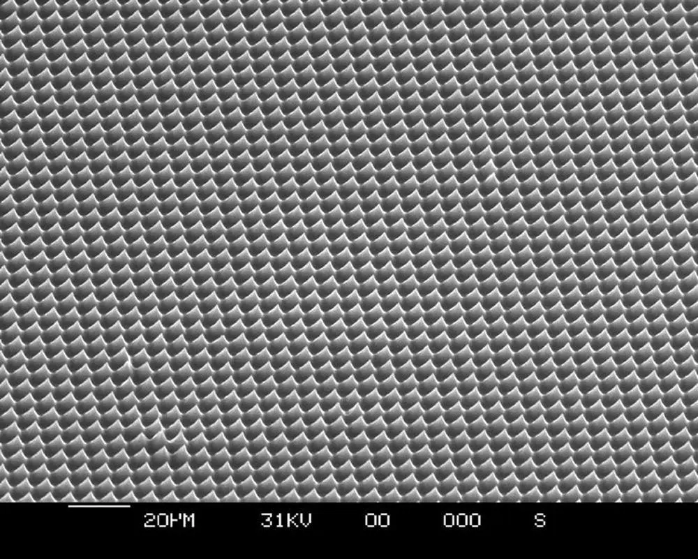
Figure 1.11 Textured (100) monocrystalline silicon wafer.
Source: Courtesy BP Archive
This was all demonstrated in the mid‐1970s, by which time research for terrestrial applications had begun and further advances in efficiency were being made for terrestrial silicon cells, as described in Chapter 4. Meanwhile, developments in space cells turned toward III–V materials, as described in section 1.4.
1.3.3 Solar Cell Manufacturing
By 1972, there were a thousand satellites in space, with power requirements which varied from milliwatts for Vanguard 1 to kilowatts for Skylab A [55]. All the attendant solar cells had to be manufactured somewhere. Initially, Hoffman Semiconductor and Western Electric supplied some, but once the application had been established, new entrants rapidly appeared, not only in the United States but also in Germany and Japan.
One of the first start‐ups in the United States was Spectrolab in 1956, which initially manufactured optical filters and mirrors but in 1958 started in the space cell business, supplying a solar array to the Explorer 1 satellite and then another to Explorer 6 in 1959. Since then, it has supplied many satellites, including for Syncom, the first successful mission in a geosynchronous orbit. In 1993, the company installed equipment for the manufacture of III–V solar cells, signalling the move way from silicon in space. It currently offers cells of 30% efficiency. In 1975, Spectrolab was acquired by Hughes Aircraft, and in 2000 it became part of Boeing Corporation. It has produced over 4 MWp of space solar cells to date, and it continues in production [56]. At the same time, the Applied Solar Energy Corporation started manufacturing space cells and pioneered the deposition of GaAs cells on germanium substrates. ASEC became Tecstar Inc., but it entered chapter 11 bankruptcy in 2002 and its assets were acquired by Emcore Inc. COMSAT, as already described, started in 1962. In Germany, AEG‐Telefunken in Heilbronn started production of space solar cells, with the first supplied to the German AZUR1 satellite in 1968 [57]. The company still produces cells today, after many changes of ownership, under the name Azur Space Solar Power GmbH. It has provided cells for over 400 space projects. In Japan, the Sharp company started research into solar cells in 1959, and specifically addressed the space market from 1967 with the first deployment in space of the Ume satellite in 1976 [58]. Sharp continues today, making triple‐junction III–V cells for both space and concentrator solar cell applications.
While manufacture of space cells continues today, it is now a relatively small market compared to the terrestrial one. However, the expertise gained in manufacturing for space provided the basis for the growth of the terrestrial market following the 1973 oil crisis, as discussed in Chapter 2. By 1970, it had already been noted that growth prospects in the space cell industry were limited, and scientists were beginning to look to earth [39]. Sharp Corporation had consistently used reject space cells for terrestrial applications, supplying photovoltaic power to 256 lighthouses between 1961 and 1972 [59]. It demonstrated the first viable silicon module for terrestrial use in 1963 and became a major supplier of photovoltaic modules from 1980 onward. AEG‐Telefunken started terrestrial solar cell manufacture at its Wedel site in the mid‐1970s [57]. Other ‘pure’ terrestrial solar cell companies were founded by individuals leaving space cell companies. Bill Yerkes had been president at Spectrolab, but following the Hughes Aircraft acquisition he left the company to form Solar Technology International, which subsequently became ARCO Solar and was the largest photovoltaics manufacturer for several years [60]. Joseph Lindmayer and Peter Varadi left COMSAT in 1973 to form the Solarex company [61], and this too – after a merger with BP Solar – became the world’s largest photovoltaics manufacturer, in 2000 [61].
In this way, the development of solar cells for space formed the foundation of the major manufacturing industry and global energy supply that photovoltaics has become.
1.4 Gallium Arsenide and III–V Alloys for Space
Despite its many advantages, silicon also has negative characteristics. Namely, it is an indirect bandgap semiconductor and the bandgap at 1.1 eV is not the optimum. This means that a relatively thick absorber layer is required to absorb the solar spectrum, and the bandgap limits the ultimate efficiency that can be achieved. The semiconductor gallium arsenide (GaAs) does not have these disadvantages. As a direct bandgap semiconductor, it requires only a few microns of absorber, which lowers the mass of the solar cell – an important characteristic in space applications. The bandgap at 1.4 eV is very near the optimum for a single‐junction solar cell [44]. GaAs also has the advantage that a wide range of alloys of various group III and V elements exist with different bandgaps and are lattice‐matched to it [62], enabling the high‐efficiency tandem structures envisaged by Jackson [43]. On the other hand, GaAs is a high‐cost technology, with the cost of substrates and active film deposition being much higher than that for silicon. Nonetheless, the cost of the solar cell is a much less important parameter than kWp/kg for space applications [63]. GaAs also has the advantage that it is more radiation‐hard than silicon [64]. GaAs cells have been used in space since the 1960s, with the Russian Venera 2 and 3 missions to Venus. In 1986, 70 m 2of GaAs solar cells were installed on the MIR space station; these functioned for 15 years [65]
The development of III–V cells can be divided into two programmes: single‐junction GaAs cells on either a GaAs substrate or germanium and tandem cells usually on a germanium substrate for use in space but also for concentrating solar cell applications. The bandgaps and lattice constants of the most important III–V compounds are given in Figure 1.12. Silicon solar cells were the preferred space cell technology until the 1990s, when III–V cells began to be used. They remain the dominant technology today.
1.4.1 Single‐Junction GaAs Solar Cells
Интервал:
Закладка:
Похожие книги на «Photovoltaics from Milliwatts to Gigawatts»
Представляем Вашему вниманию похожие книги на «Photovoltaics from Milliwatts to Gigawatts» списком для выбора. Мы отобрали схожую по названию и смыслу литературу в надежде предоставить читателям больше вариантов отыскать новые, интересные, ещё непрочитанные произведения.


Обсуждение, отзывы о книге «Photovoltaics from Milliwatts to Gigawatts» и просто собственные мнения читателей. Оставьте ваши комментарии, напишите, что Вы думаете о произведении, его смысле или главных героях. Укажите что конкретно понравилось, а что нет, и почему Вы так считаете.