Design and Development of Efficient Energy Systems
Здесь есть возможность читать онлайн «Design and Development of Efficient Energy Systems» — ознакомительный отрывок электронной книги совершенно бесплатно, а после прочтения отрывка купить полную версию. В некоторых случаях можно слушать аудио, скачать через торрент в формате fb2 и присутствует краткое содержание. Жанр: unrecognised, на английском языке. Описание произведения, (предисловие) а так же отзывы посетителей доступны на портале библиотеки ЛибКат.
- Название:Design and Development of Efficient Energy Systems
- Автор:
- Жанр:
- Год:неизвестен
- ISBN:нет данных
- Рейтинг книги:5 / 5. Голосов: 1
-
Избранное:Добавить в избранное
- Отзывы:
-
Ваша оценка:
Design and Development of Efficient Energy Systems: краткое содержание, описание и аннотация
Предлагаем к чтению аннотацию, описание, краткое содержание или предисловие (зависит от того, что написал сам автор книги «Design and Development of Efficient Energy Systems»). Если вы не нашли необходимую информацию о книге — напишите в комментариях, мы постараемся отыскать её.
This volume is focused on saving energy at different levels of design and automation including the concept of machine learning automation and prediction modeling. It also deals with the design and analysis for IoT-enabled systems including energy saving aspects at different level of operation.
The editors and contributors also cover the fundamental concepts of IoT and machine learning, including the latest research, technological developments, and practical applications. Valuable as a learning tool for beginners in this area as well as a daily reference for engineers and scientists working in the area of IoT and machine technology, this is a must-have for any library.
Design and Development of Efficient Energy Systems — читать онлайн ознакомительный отрывок
Ниже представлен текст книги, разбитый по страницам. Система сохранения места последней прочитанной страницы, позволяет с удобством читать онлайн бесплатно книгу «Design and Development of Efficient Energy Systems», без необходимости каждый раз заново искать на чём Вы остановились. Поставьте закладку, и сможете в любой момент перейти на страницу, на которой закончили чтение.
Интервал:
Закладка:
Figure 1.4shows the performance of MOSFET when different gate contacts are used like aluminium, polysilicon and copper. MOSFET shows better performance when polysilicon is used as a gate contact. Metal gates like Aluminium and copper operate at voltages 3V to 5V. The lowering of operating voltages leads to the use of polysilicon gate contact. From the graph we can observe at lower operating voltages polysilicon gate contact gives better performance because the OFF-state current is low.
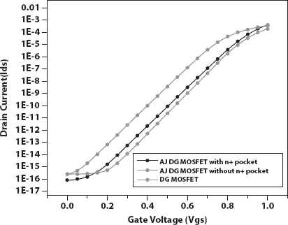
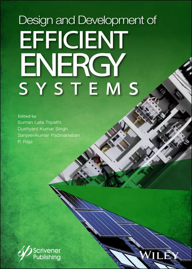
Figure 1.2 I dversus V gsplot of AJ-DGMOSFET.
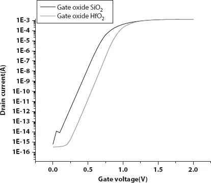
Figure 1.3Id Versus Vgs plot with different oxide region material.
The proposed JL-DG MOSFET has ratio of 10 13which is higher than other existing structures. The calculation of SCE parameters like SS and DIBL is also a deciding factor for device performance. The proposed device show SS value of 59 mV/ decade and DIBL of 13.4 mV/V. Both SS and DIBL values are less than other existing transistors. Therefore, heavily doped AJ-DG MOSFET has superior ON/OFF performances.
Figure 1.4 I dversus V gsPlot of different gate contact material.
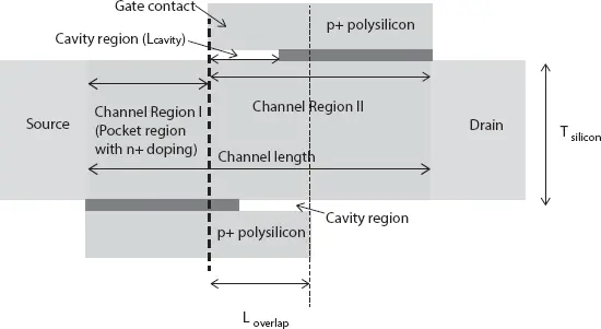
Figure 1.5 JL-DG MOSFET with cavity region.
1.5 Heavily Doped JL-DG MOSFET for Biomedical Application
DG MOSFETs were designed with a nanogap cavity region as bio-sensor that can sense the bio-molecule present in the nanogap cavity [23, 24]. These bio-sensors work on the principle of dielectric modulation with the variation in bio-species present in the air (nanogap cavity) that further varies the electrical parameters of the device.
Figure 1.5shows the 2-D view of JL-DG MOSFET with a cavity region. Here the cavity plays an important role to sense the bio-species present in air. The presence of bio-species and their concentration affect the dielectric constant of the cavity region that further affects the electrical parameters of transistor. The cavity region with different length (L cavity) and height (H cavity) shows varied device sensitivity towards the presences of biomolecules. This effect has been studied through varying dielectric constant with different materials such as air, SiO 2, HfO 2and S 3 N 4.
Figure 1.5shows AJ-DG MOSFET with the nanogap cavity region. A thin SiO 2layer used for binding the molecules entering the cavity region by restricting the movements of bio-molecules. For the presented device the cavity region height (H cavity) is 2.7 nm and SiO 2layer thickness is 0.3 nm. Another way to analyze device sensitivity is by introducing different types of charged particles in the cavity region.
In Figure 1.6a sharp change is observed in the threshold voltages with the different dielectric constant of the material added in the cavity region. The longer cavity region length shows more variations in threshold voltage that results in the shifting of channel inversion threshold level. Therefore with a higher value of dielectric constant, the threshold voltage lowers. This shows that the device is highly sensitive towards the change in dielectric material constant depending on biomolecule presence resulting in electrical parameter variations.
A significant variation in threshold voltage is observed with a change in oxide thickness. The changing oxide thickness results in a change in the cavity region thickness that also affects the electrical parameter variations.
1.6 Conclusion
The AJ-DG MOSFET is a suitable choice for low-power applications such as bulk memories that are integral parts of many IoT-enabled systems. The performance of AJ-DG MOSFET can also be varied by adjusting the position of the top and bottom gate overlapping regions. High ON/OFF current ratio and low leakage current are the key features of the AJ-DG MOSFET with low static power consumption and enhanced speed of circuit operation. Another application of JL-DG MOSFET is as biosensor by introducing cavity region between gate and channel. These cavity regions are sensitive to the bio species present in the environment. The variation in biomolecule changes the dielectric constant of the medium that results in the variation in electrical parameters of a device that can be easily measured to detect the presence of bio-species.
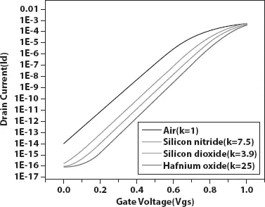
Figure 1.6 I dVersus V gsof AJ-DG MOSFET with varying dielectric constant (Lcavity = 7nm).
References
1. S L Tripathi, Ramanuj Mishra, R A Mishra, “Characteristic comparison of connected DG FINFET, TG FINFET and Independent Gate FINFET on 32 nm technology” IEEE ICPCES , pp. 1-7, December, 2012.
2. Ammina, V.P., Vankudothu, S.P., Shaik, R.R. et al. An Optimized Ge Pocket SOI JLT with Efforts to Improve the Self-Heating Effect: Doping & Materials Perspective. Silicon, 2019. https://doi.org/10.1007/s12633-019-00319-x
3. F. Djeffal, H.Ferhat, T.Bentrcia .Improved analog and RF performances of gate-all-around junctionless MOSFET with drain and source extensions, Superlattices and Microstructures, 90, 132-140, 2016.
4. Nirmal Ch. Roy, Abhinav Gupta, Sanjeev Rai. Analytical surface potential modeling and simulation of junction-less double gate (JLDG) MOSFET for ultra low-power analog/RF circuits, Microelectronics Journal, 46 (10), 916-922, 2015.
5. E. Chebaki, F.Djeffal ,H.Ferhati, T.Bentrcia. Improved analog/RF performance of double gate junctionless MOSFET using both gate material engineering and drain/source extensions, Superlattices and Microstructures, 92, 80-91, 2016.
6. Ali A. Orouji, M. Jagdeesh. Nanoscale SOI MOSFETs with electrically induced source/drain extension: Novel attributes and design considerations for suppressed short-channel effects, Superlattices and Microstructures, 39(5), 395-405, 2006.
7. Ajay, Rakhi Narang ,Manoj Saxena ,Mridula Gupta. Investigation of dielectric modulated (DM) double gate (DG) junctionless MOSFETs for application as a biosensors, Superlattices and Microstructures , 85, 557-572, 2015.
8. Varsha Pathak, Gaurav Saini. A Graded Channel Dual-Material Gate Junctionless MOSFET for Analog Applications, Procedia Computer Science, Vol. 125, 825-831, 2018.
9. Ajay Kumar, M.M.Tripathi, Rishu Chaujar. Analysis of sub-20 nm black phosphorus based junctionless-recessed channel MOSFET for analog/RF applications, Superlattices and Microstructures , 116, April 171-180, 2018.
10. Angsuman Sarkar, Aloke Kumar Das ,Swapnadip De, Chandan Kumar Sarkar. Effect of gate engineering in double-gate MOSFETs for analog/RF applications, Microelectronics Journal, 43(11), 873-882, 2012.
11. Yon-Sup Pang, John R Brews. Design of 0.1-lm pocket n-MOSFETs for low-voltage applications , Solid-State Electronics, 46(12), 2315-2322 , 2002.
Читать дальшеИнтервал:
Закладка:
Похожие книги на «Design and Development of Efficient Energy Systems»
Представляем Вашему вниманию похожие книги на «Design and Development of Efficient Energy Systems» списком для выбора. Мы отобрали схожую по названию и смыслу литературу в надежде предоставить читателям больше вариантов отыскать новые, интересные, ещё непрочитанные произведения.


Обсуждение, отзывы о книге «Design and Development of Efficient Energy Systems» и просто собственные мнения читателей. Оставьте ваши комментарии, напишите, что Вы думаете о произведении, его смысле или главных героях. Укажите что конкретно понравилось, а что нет, и почему Вы так считаете.