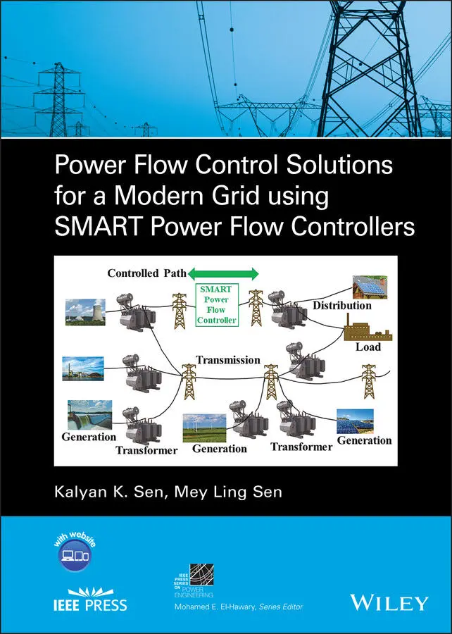
Kalyan K. Sen - Power Flow Control Solutions for a Modern Grid Using SMART Power Flow Controllers
Здесь есть возможность читать онлайн «Kalyan K. Sen - Power Flow Control Solutions for a Modern Grid Using SMART Power Flow Controllers» — ознакомительный отрывок электронной книги совершенно бесплатно, а после прочтения отрывка купить полную версию. В некоторых случаях можно слушать аудио, скачать через торрент в формате fb2 и присутствует краткое содержание. Жанр: unrecognised, на английском языке. Описание произведения, (предисловие) а так же отзывы посетителей доступны на портале библиотеки ЛибКат.
- Название:Power Flow Control Solutions for a Modern Grid Using SMART Power Flow Controllers
- Автор:
- Жанр:
- Год:неизвестен
- ISBN:нет данных
- Рейтинг книги:5 / 5. Голосов: 1
-
Избранное:Добавить в избранное
- Отзывы:
-
Ваша оценка:
Power Flow Control Solutions for a Modern Grid Using SMART Power Flow Controllers: краткое содержание, описание и аннотация
Предлагаем к чтению аннотацию, описание, краткое содержание или предисловие (зависит от того, что написал сам автор книги «Power Flow Control Solutions for a Modern Grid Using SMART Power Flow Controllers»). Если вы не нашли необходимую информацию о книге — напишите в комментариях, мы постараемся отыскать её.
Power Flow Control Solutions for a Modern Grid using SMART Power Flow Controllers
Power Flow Control Solutions for a Modern Grid using SMART Power Flow Controllers
Power Flow Control Solutions for a Modern Grid Using SMART Power Flow Controllers — читать онлайн ознакомительный отрывок
Ниже представлен текст книги, разбитый по страницам. Система сохранения места последней прочитанной страницы, позволяет с удобством читать онлайн бесплатно книгу «Power Flow Control Solutions for a Modern Grid Using SMART Power Flow Controllers», без необходимости каждый раз заново искать на чём Вы остановились. Поставьте закладку, и сможете в любой момент перейти на страницу, на которой закончили чтение.
Интервал:
Закладка:
The direct way to modify the effective line reactance ( jX eff) between its two ends is to connect a compensating reactance (– jX se) in series with the line as shown in Figure 1-6. The active and reactive power flows ( P rand Q r) at the receiving end of the line are given by the following equations:
(2‐207) 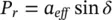
and
(2‐208) 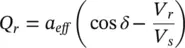
where
(2‐209) 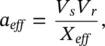
(2‐210a) 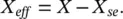
Note that X se> 0 represents a capacitive compensating reactance and X se< 0 represents an inductive compensating reactance, respectively. However, X eff> 0 represents an effective inductive reactance and X eff< 0 represents an effective capacitive reactance, respectively.
Figure 1-6 Power flow in a lossless line with a series‐compensating reactance ( X se).
Depending on whether the compensating reactance (– jX se) is capacitive or inductive, the voltage ( V q= jV q) across the compensating reactance lags or leads the prevailing line current ( I) by 90°. This leads to the concept of an emulated reactance, which is defined as
(1‐3a) 
or
(1‐3b) 
and is shown in Figure 1-7. In this concept, a compensating voltage  is created, maintaining the quadrature relationship with the prevailing line current, and is connected in series with the line. Note that
  is defined to be a capacitive compensation and V s′s< 0 is defined to be an inductive compensation, respectively.
The concept of an emulated reactance can be further extended to represent an emulated impedance when the compensating voltage is not restricted to be in quadrature, but at any phase angle with respect to the prevailing line current ( I). That means the compensating voltage  can be made to look like a virtual, four‐quadrant, compensating impedance ( Z se= R se− jX se) that consists of a resistance ( R se= + R or − R ) and a reactance ( X se= X Cor − X L) in series with the line without any discrete circuit component as shown in Figure 1-8b. This two‐parameter, resistive ( R se) and reactive ( X se), control makes it possible to modify the magnitude and the phase angle of the line voltage simultaneously, which results in an independent control of active and reactive power flows in the line.
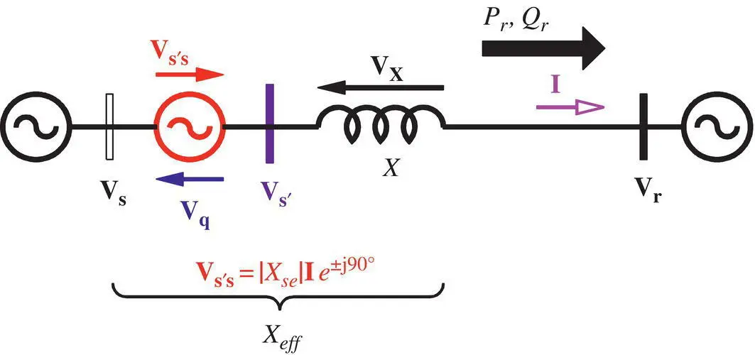
Figure 1-7 Power flow in a lossless line with a series‐compensating voltage ( V s′s).
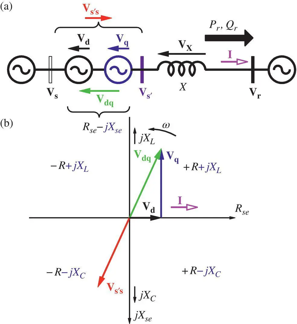
Figure 1-8 (a) Power transmission system with a series‐compensating voltage ( V s′s); (b) four‐quadrant emulated impedance.
The series‐compensating voltage ( V s′s) is related to ( V dq), such that
(1‐4) 
and
(1‐5) 
where V d= V dand V q= jV qare the respective active or direct and reactive or quadrature components of the compensating voltage with load convention, meaning the line current ( I) enters at the higher potential terminal of the voltages ( V dand V q) as shown in Figure 1-8a.
The natural or uncompensated power flow through a transmission line in a power system network is, in general, not optimal. Any of the power flow control parameters (line voltage magnitude, its phase angle, and line reactance) can be regulated with the use of the following equipment:
Voltage‐Regulating Transformer (VRT), shunt or parallel‐connected switched reactor/capacitor, also known as Shunt Reactor (SR)/Shunt Capacitor (SC), Static Var Compensator (SVC), or STATic synchronous COMpensator (STATCOM) for voltage regulation as shown in Figure 1-9
PAR or Phase‐Shifting Transformer (PST) for phase angle regulation as shown in Figure 1-10
Thyristor‐Controlled Series Capacitor (TCSC) or Static Synchronous Series Compensator (SSSC) for series reactance regulation as shown in Figure 1-11.
The dynamic performance of a VRT is limited by the speed of operation of the mechanical Load Tap Changers (LTCs), which respond in seconds; this level of response time is acceptable in most utility applications. However, if a faster response is desired, the mechanical LTCs can be upgraded with power electronics‐based LTCs, called Thyristor‐Controlled (TC) LTCs as discussed in Chapter 2. More on LTCs can be found in the book, titled “On‐Load Tap‐Changers For Power Transformers: Operation, Principles, Applications and Selection,” by A. Krämer, Maschinenfabrik Reinhausen, 2000. The power electronics‐based solutions can be divided into two categories, based on the type of semiconductor switches: naturally commutated switch, such as a thyristor and forced‐commutated switch, such as Insulated Gate Bipolar Transistor (IGBT). Each of these solutions is based on engineering trade‐offs.
Читать дальшеИнтервал:
Закладка:
Похожие книги на «Power Flow Control Solutions for a Modern Grid Using SMART Power Flow Controllers»
Представляем Вашему вниманию похожие книги на «Power Flow Control Solutions for a Modern Grid Using SMART Power Flow Controllers» списком для выбора. Мы отобрали схожую по названию и смыслу литературу в надежде предоставить читателям больше вариантов отыскать новые, интересные, ещё непрочитанные произведения.


Обсуждение, отзывы о книге «Power Flow Control Solutions for a Modern Grid Using SMART Power Flow Controllers» и просто собственные мнения читателей. Оставьте ваши комментарии, напишите, что Вы думаете о произведении, его смысле или главных героях. Укажите что конкретно понравилось, а что нет, и почему Вы так считаете.