John Crisp - Introduction to Microprocessors and Microcontrollers
Здесь есть возможность читать онлайн «John Crisp - Introduction to Microprocessors and Microcontrollers» весь текст электронной книги совершенно бесплатно (целиком полную версию без сокращений). В некоторых случаях можно слушать аудио, скачать через торрент в формате fb2 и присутствует краткое содержание. Год выпуска: 2004, ISBN: 2004, Издательство: Elsevier, Жанр: Компьютерное железо, на английском языке. Описание произведения, (предисловие) а так же отзывы посетителей доступны на портале библиотеки ЛибКат.
- Название:Introduction to Microprocessors and Microcontrollers
- Автор:
- Издательство:Elsevier
- Жанр:
- Год:2004
- ISBN:0-7506-5989-0
- Рейтинг книги:3 / 5. Голосов: 1
-
Избранное:Добавить в избранное
- Отзывы:
-
Ваша оценка:
Introduction to Microprocessors and Microcontrollers: краткое содержание, описание и аннотация
Предлагаем к чтению аннотацию, описание, краткое содержание или предисловие (зависит от того, что написал сам автор книги «Introduction to Microprocessors and Microcontrollers»). Если вы не нашли необходимую информацию о книге — напишите в комментариях, мы постараемся отыскать её.
Introduction to Microprocessors and Microcontrollers — читать онлайн бесплатно полную книгу (весь текст) целиком
Ниже представлен текст книги, разбитый по страницам. Система сохранения места последней прочитанной страницы, позволяет с удобством читать онлайн бесплатно книгу «Introduction to Microprocessors and Microcontrollers», без необходимости каждый раз заново искать на чём Вы остановились. Поставьте закладку, и сможете в любой момент перейти на страницу, на которой закончили чтение.
Интервал:
Закладка:
Power supplies
The main power supplies to operate the chip are the +5 V applied to the V+ pin and 0 V on the GND (ground) pin.
To program the memory, the programming voltage is applied to Vpp. When not being programmed, it should be held at +5 V. Be careful to read the data book – the value of Vpp differs widely.
Address pins
Address pins are always numbered starting from A0. We have seen that the number of location is given by 2 n so with 17 address lines (A0 to A16) the number of locations would be 2 17=131 072.
Data pins
Like the addresses, these pins always start counting from zero. In the EPROM shown in Figure 6.19, they are abbreviated to D for data and go from D0 to D7 – eight in all. Some manufacturers call them output pins and number them O0, O1, O2 etc. The output from these pins is either 0 V or +5 V or near to these values.
Control pins
1 Chip enable (CE), sometimes called chip select (CS), is the main on/off switch for the chip. It is usually active low, which means that the chip needs a logic 0 voltage to be applied to switch the chip on. This is indicated by a line over the CE. When the chip is switched off, it goes to sleep and the power drops with a reduction of about 150 times.
2 Output enable (OE) leaves the chip fired up but with its output disconnected from the data pins. This is done by disabling a series of tri-state buffers immediately before the data pins. Disconnecting the output pins is very much faster than switching the chip off. Watch out for the line over the name to indicate the polarities required.
Unconnected pins
These are shown as NC and are not used. They are physically separate from the internal chip and therefore have no effect of anything. They should be left unconnected.
Have a look at the SRAM in Figure 6.20. Many of these pins will be recognized as being the same as we saw with the EPROM.
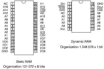
Figure 6.20 Pin out diagrams of RAM chips
Data pins
Since the SRAM is a read/write memory, the data pins are used to read data into the chip and to write data out to the microprocessor system. With this in mind, they have been called input/output pins (I/O) and, as usual, are numbered from zero.
Control pins
1 Write enable (WE#) controls internal tri-state buffers to control the flow of data to write or read on the data pins. The line over the WE indicates that, to write data, the pin must be held low. 2 There are two chip selects, one shown as active low and one as active high. To enable the chip, both must have the correct voltage present. This provides a degree of flexibility to the system designer. If either is not required, it can simply be held down permanently to its appropriate voltage and then the other can then be used to control the operation of the chip.
Row address strobe (RAS) and Column address strobe (CAS)
At first glance, there does not seem to be enough address pins for the number of locations to be addressed. A0 to A9 is only 10 pins, which would suggest a total of 2 10or 1024 locations. The trick here is to use the same pins twice and hence load in a total 220 or 1 048 576 addresses.
The sequence of events dictates that the RAS line is taken low and the bottom half of the address is loaded into the Rows – RAS then returns high. Then the CAS is taken low while the remainder of the address is fed into the columns. After this, the state of the write line (same as R/W) determines whether data is entering or leaving the DRAM.
There is only a single bit stored in each address, the data entering via the data in (Din) pin and leaving via the data out (Dout) pin.
SIMMs
Single in-line memory modules are a collection of separate RAM chips that are mounted on a piece of board to make installation quicker and easier. They are not actually a different type of memory.
RAM Cards
The problem with RAM memory is that it is volatile. The information is lost as soon as the system is switched off. RAM cards overcome this by providing the RAM chips with their own on-board battery. In this way, the RAM card can be removed from the system without losing the data. It is really a RAM pretending to be ROM. This provides full speed operation and permanence during the 10-year life of the battery.
Flash memory
This is non-volatile RAM (NVRAM). In fact, it is really a form of RAM with a battery installed to provide power during shutdown periods. Rather like a single chip version of a RAM card.
A microprocessor has a number of address lines that can be used to access RAM or ROM or other devices within the system. As we saw in the memory chips, the total memory addressable by a microprocessor is found by the formula 2 n where n is the number of address lines. For example, an 8-bit microprocessor generally has 16 address lines and can access 2 16or would have 65 536 or 64 bytes of memory. The Digital Alpha 21064 has 34-bit address lines giving 2 34or a little over 17 Gbytes. This memory is shared between the RAMs, ROMs and other devices, including some for the microprocessor itself to use.
The system designer has to decide in what way the available memory is to be used. Using the memory map of the 8-bit microprocessor as a simple example, we start off with a blank space as in Figure 6.21. When the microprocessor is first supplied with power it will immediately start following the first program provided. How does it know what program is first? The answer to this is that it goes to a predetermined address, which has been built into the microprocessor during manufacture.
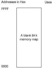
Figure 6.21 The starting point for a memory map
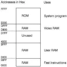
Figure 6.22 A typical small system memory map
If we assume the startup address is FFFAH, then we must put some useful information at that address for it to follow. This implies that some ROM memory must be at the top end of the memory map. Most provide some extra fast programming ability and this usually requires that some RAM to be available at the bottom end of the memory map.
There is nothing else that is allocated to any particular address so any other RAM and ROM memories can be placed at any position on the map. The map does not have to be full, indeed it seldom is. The balance between RAM and ROM depends on the purpose to which the system is to be put. A control system running a piece of manufacturing machinery is likely to be predominately ROM whereas a computer would need significant RAM. A simple memory map is shown in Figure 6.22.
Sorting out the addresses
This is just an exercise in hex numbers in which a ‘hex’ calculator will prove invaluable. Now, 1 kbyte of memory occupies 2 10or 1024 locations, which is 400H in hex. The first section of RAM extends from: start address + highest RAM address = 0000H to 03FFH so the highest address in the ‘Fast instructions’ section is 03FFH. The User RAM extends from 0400H to 3FFFH. How many kilobytes of memory is this?
This is 15 kbytes of memory. This was found by subtracting 0400H from 4000H to give 3C00H and then dividing this result by 400H, the hex equivalent of 1 kbyte. The division is best done by calculator. Remember that the fact that the user-RAM ended at 3FFFH means that the total number of locations, including the first one in 4000H so it was more convenient to use the figure of 4000H straight from the memory map. This is sometimes a little difficult to fully come to terms with, but a cup of coffee and a slump in an armchair often helps.
Читать дальшеИнтервал:
Закладка:
Похожие книги на «Introduction to Microprocessors and Microcontrollers»
Представляем Вашему вниманию похожие книги на «Introduction to Microprocessors and Microcontrollers» списком для выбора. Мы отобрали схожую по названию и смыслу литературу в надежде предоставить читателям больше вариантов отыскать новые, интересные, ещё непрочитанные произведения.


Обсуждение, отзывы о книге «Introduction to Microprocessors and Microcontrollers» и просто собственные мнения читателей. Оставьте ваши комментарии, напишите, что Вы думаете о произведении, его смысле или главных героях. Укажите что конкретно понравилось, а что нет, и почему Вы так считаете.