2D Monoelements
Здесь есть возможность читать онлайн «2D Monoelements» — ознакомительный отрывок электронной книги совершенно бесплатно, а после прочтения отрывка купить полную версию. В некоторых случаях можно слушать аудио, скачать через торрент в формате fb2 и присутствует краткое содержание. Жанр: unrecognised, на английском языке. Описание произведения, (предисловие) а так же отзывы посетителей доступны на портале библиотеки ЛибКат.

- Название:2D Monoelements
- Автор:
- Жанр:
- Год:неизвестен
- ISBN:нет данных
- Рейтинг книги:5 / 5. Голосов: 1
-
Избранное:Добавить в избранное
- Отзывы:
-
Ваша оценка:
2D Monoelements: краткое содержание, описание и аннотация
Предлагаем к чтению аннотацию, описание, краткое содержание или предисловие (зависит от того, что написал сам автор книги «2D Monoelements»). Если вы не нашли необходимую информацию о книге — напишите в комментариях, мы постараемся отыскать её.
Recent advances in phosphorene The diverse properties of two-dimensional antimonene, of graphene and its derivatives The molecular docking simulation study used to analyze the binding mechanisms of graphene oxide as a cancer drug carrier Metal-organic frameworks (MOFs)-derived carbon (graphene and carbon nanotubes) and MOF-carbon composite materials, with a special emphasis on the use of these nanostructures for energy storage devices (supercapacitors) Two-dimensional monoelements classification like graphene application in field-effect transistors for sensing and biosensing Graphene-based ternary materials as a supercapacitor electrode Rise of silicene and its applications in gas sensing
2D Monoelements — читать онлайн ознакомительный отрывок
Ниже представлен текст книги, разбитый по страницам. Система сохранения места последней прочитанной страницы, позволяет с удобством читать онлайн бесплатно книгу «2D Monoelements», без необходимости каждый раз заново искать на чём Вы остановились. Поставьте закладку, и сможете в любой момент перейти на страницу, на которой закончили чтение.
Интервал:
Закладка:
In particular, there are no dangling bonds in 2D materials, thus the 2D materials can also be employed as the substrates to grow antimonene. Sun et al. grew a series of antimonene (Sb) with various morphs on two types of single-crystalline graphene substrates by the vdWE method [26]. One of the substrates was the as-grown graphene on Cu (111)/ c -sapphire via chemical vapor deposition (CVD), and another was the transferred graphene on SiO 2/Si. On the as-grown graphene, triangle Sb islands (up-pointing and down-pointing triangles) were grown in Volmer-Weber (VW) modes with height of ~17.5 ± 0.7 nm, while Sb sheets were grown in Frank-van der Merve (FM) modes with height of ~4.5 ± 0.7 nm ( Figure 2.5e). The growth of Sb sheets was probably caused by the remote epitaxy between Sb and underlying Cu. The epitaxial alignments between Sb (0001) and graphene were different in various morphs of Sb, i.e., Sb [1i00]∥graphene [10] and [10i0]∥graphene [10] for up-pointing and down-pointing Sb islands, [2ii0]∥graphene [10] for Sb sheets ( Figure 2.5f). In contrast, only VW growth of Sb islands was found on the transferred graphene due to the absence of Cu. In addition, high-quality Sb thin films were also grown on both substrates, and these two films showed no significant difference. The epitaxial alignment in Sb thin films was the same as that in Sb islands. In another work, β-antimonene was also grown on WSe 2substrate to form the Sb/WSe 2heterostructure through van der Waals interactions [27].
The earliest MBE growth of antimonene was reported by T. Lei et al. in 2016 [28]. In this work, bilayer antimonene was grown smoothly on 3D topologically insulated Bi 2Te 3(111) and Sb 2Te 3(111) substrates with small lattice mismatch. The clear low-energy electron diffraction (LEED) pattern indicated the 1 × 1 periodicity of the antimonene/Sb 2Te 3(111) surface, showing that high-quality epitaxial antimonene was formed. The surface states of MBE grown antimonene were probed by angle-resolved photoemission spectroscopy (ARPES), and it showed similar electronic structures on the surfaces of two substrates, but the bands of antimonene on Bi 2Te 3(111) surface were flatter than on Sb 2Te 3(111) surface due to the larger lattice constants of Bi 2Te 3(111) substrate. The interfacial strain and charge transfer induced a change in band dispersions. This work is a milestone in this kind of study, which is critical for the understanding of the electrical structure of antimonene.
Subsequently, monolayer-to-multilayer antimonene were successfully grown on 2D substrates by the MBE method, such as PdTe 2, MoS 2, WTe 2, and graphene [29–32]. Wu et al. grew large-area monolayer antimonene on a freshly cleaved PdTe 2substrate in an ultrahigh vacuum (UHV) MBE chamber (2 × 10 −10mbar), and the schematic of growth process was shown in Figure 2.6a[29]. 2D PdTe 2was chosen as a suitable substrate in the growth of antimonene, because of its small mismatch of crystal periodicity with free-standing antimonene and chemically stable surface. From the topological scanning tunneling microscopy (STM) image shown in Figure 2.6b, it is observed that an atomically smooth antimonene film was obtained with no obvious defects or domain boundaries. According to the LEED pattern in the inset of Figure 2.6b, this film is a well-ordered single crystalline with a commensurate (1 × 1) lattice periodicity. The height of this film is about 2.8 Å, which is consistent with that of a monolayer antimonene ( Figure 2.6c). Figure 2.6dshows an atomic-resolution STM image of antimonene, it is clearly seen that this epitaxial film has a buckled honeycomb lattice with a periodicity of 4.13 ± 0.02 Å. It is noted that monolayer antimonene grown on PdTe 2was chemically inert to the air. This work first unveils the atomic-scale morphology of epitaxial monolayer β-antimonene.
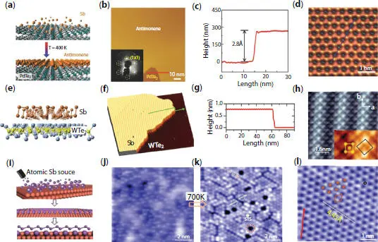
Figure 2.6 (a) Schematic of growth process of monolayer antimonene on 2D PdTe 2substrate. (b) Topographic STM image of large-area antimonene on PdTe 2. Inset: LEED pattern of monolayer antimonene on PdTe 2substrate. (c) A height profile of antimonene taken along the red line in panel (b). (d) Atomic-resolution STM image of antimonene. (e) Schematic diagram of epitaxial α-antimonene on 2D Td-WTe 2substrate. (f) Topographic STM image of monolayer α-antimonene on WTe 2. The area is 120 × 120 nm 2. (g) A line-scan profile of antimonene along the green line in panel (f). (h) Atomic-resolution STM image taken at U = +300 mV, I t= 100 pA. The area is 8 × 8 nm 2. Inset: the unit cells of √2 × √2 lattice and original 1 × 1 lattice. (i) Schematic of the evolution processes from initial Sb atoms to final antimonene on Cu (111) substrates. Topographic STM images of 0.5 monolayer antimonene deposition on Cu (111) surface before (j) and (k) after annealing at 700 K. (l) High-resolution STM image of antimonene. (a–d) Reproduced with permission [29]. Copyright 2017, Wiley-VCH. (e–h) Reproduced with permission [30]. Copyright 2019, Wiley-VCH. (i–l) Reproduced with permission [36]. Copyright 2019, Wiley-VCH.
Interestingly, besides the usual β-antimonene, α-phase antimonene can also be obtained on the 2D substrate by using MBE. Shi et al. controllably synthesized micro-sized monolayer α-antimonene on the 2D T d-WTe 2substrate [30]. Due to the inert surface and the compatibility with α-antimonene, T d-WTe 2was considered as a suitable substrate to achieve the freestanding epitaxial growth of monolayer α-antimonene. As illustrated in Figure 2.6e, α-antimonene takes a BP-like puckered honeycomb structure, which is different from a buckled honeycomb structure of β-antimonene. Figure 2.6fshows the topographic STM image of α-antimonene, it can be seen that Sb forms atomically flat islands on the T d-WTe 2with no apparent defects, and the height of the Sb island is around 0.78 nm ( Figure 2.6g). The atomic-resolution STM image ( Figure 2.6h) revealed a reconstructed √2 √2 lattice of α-antimonene with lattice constants of 0.62 × 0.63 nm. Monolayer α-antimonene possesses a linearly dispersed metallic band crossing the Fermi level, resulting in a high electrical conductivity. Large-scale multilayer antimonene was also grown by controlling the amount of Sb, which showed ultrahigh stability in air.
In the meantime, MBE was employed to grow antimonene on different metal substrates as well, including Ge (111), Ag (111), Pd (111), Cu (110), and Cu (111) [33–36]. Niu et al. fabricated single-crystalline monolayer antimonene on Cu (111) and Cu (110) substrates via MBE [36]. When Sb atoms were deposited on two substrates at low coverage, surface alloys were first formed, including √3 × √3 R30°-Sb on Cu (111) and c (2 × 2)-Sb on Cu (110). After increasing the coverage to 1 monolayer followed by postannealing, two atomic types of monolayer antimonene were then formed. Schematic of epitaxial growth of Sb atoms on Cu (111) substrates was shown in Figure 2.6i, where Sb atoms were evaporated from a Knudsen cell onto clean Cu (111) surfaces held at room temperature in an UHV chamber (2 × 10 −10mbar). The topographic STM image of 0.5 monolayer antimonene illustrated that Cu (111) surface was covered by short-range ordered single Sb atoms and their small clusters ( Figure 2.6j). After annealing at 700 K, a variety of patches with dark holes (missing atoms) and black lines (misalignment of neighboring domains) were generated ( Figure 2.6k). When increasing the coverage and postannealing, well-ordered monolayer antimonene was formed, showing a buckled honeycomb lattice and a larger lattice constant than the free-standing antimonene because of a 7.5% tensile strain ( Figure 2.6l). But unlike the result of Cu (111) surface, threefold symmetric antimonene was formed on the twofold symmetric c (2 × 2) Sb-Cu (110) surface, inducing a 6.8% compressive strain. The generation of strain also caused the changes of band gaps of antimonene on two substrates.
Читать дальшеИнтервал:
Закладка:
Обсуждение, отзывы о книге «2D Monoelements» и просто собственные мнения читателей. Оставьте ваши комментарии, напишите, что Вы думаете о произведении, его смысле или главных героях. Укажите что конкретно понравилось, а что нет, и почему Вы так считаете.