Green Energy
Здесь есть возможность читать онлайн «Green Energy» — ознакомительный отрывок электронной книги совершенно бесплатно, а после прочтения отрывка купить полную версию. В некоторых случаях можно слушать аудио, скачать через торрент в формате fb2 и присутствует краткое содержание. Жанр: unrecognised, на английском языке. Описание произведения, (предисловие) а так же отзывы посетителей доступны на портале библиотеки ЛибКат.
- Название:Green Energy
- Автор:
- Жанр:
- Год:неизвестен
- ISBN:нет данных
- Рейтинг книги:3 / 5. Голосов: 1
-
Избранное:Добавить в избранное
- Отзывы:
-
Ваша оценка:
Green Energy: краткое содержание, описание и аннотация
Предлагаем к чтению аннотацию, описание, краткое содержание или предисловие (зависит от того, что написал сам автор книги «Green Energy»). Если вы не нашли необходимую информацию о книге — напишите в комментариях, мы постараемся отыскать её.
To maintain the supply for electrical energy, researchers, engineers and other professionals in industry are continuously exploring new eco-friendly energy technologies and power electronics, such as solar, wind, tidal, wave, bioenergy, and fuel cells. These technologies have changed the concepts of thermal, hydro and nuclear energy resources by the adaption of power electronics advancement and revolutionary development in lower manufacturing cost for semiconductors with long time reliability. The latest developments in renewable resources have proved their potential to boost the economy of any country.
Green energy technology has not only proved the concept of clean energy but also reduces the dependencies on fossil fuel for electricity generation through smart power electronics integration. Also, endless resources have more potential to cope with the requirements of smart building and smart city concepts. A valuable reference for engineers, scientists, chemists, and students, this volume is applicable to many different fields, across many different industries, at all levels. It is a must-have for any library.
Green Energy — читать онлайн ознакомительный отрывок
Ниже представлен текст книги, разбитый по страницам. Система сохранения места последней прочитанной страницы, позволяет с удобством читать онлайн бесплатно книгу «Green Energy», без необходимости каждый раз заново искать на чём Вы остановились. Поставьте закладку, и сможете в любой момент перейти на страницу, на которой закончили чтение.
Интервал:
Закладка:
In forward biasing mode, an electric field forces free electrons in n- type block and holes in p- type block towards the depletion region. In this biasing, holes and free electrons recombine with ions in the depletion region to reduce the width of the depletion region. On increasing the forward voltage further, depletion region becomes thinner and a larger number of majority carriers are able to pass through the barrier. It needs to be pointed out that no net current flows in the diode in absence of an externally applied electric field.
1.1.3.1 Equilibrium Fermi Energy (EF)
In the state of thermal equilibrium, the individual hole and electron streams passing through the barrier are ideally zero. The state of thermal equilibrium can be defined as the steady-state condition at a given temperature when no externally applied field is present. In this case, the net current density due to both drift and diffusion currents should be zero for both holes and electrons. Thus, net current density for holes is given as [10,11,23,24],
(1.1) 
(1.2) 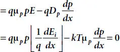
where,  is the Einstein relation. Also,
The expression for hole concentration,
(1.3) 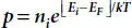
Differentiating equation (1.3)with respect to x in the equilibrium condition, 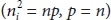
(1.4) 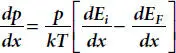
From equation (1.2)with the help of equation (1.4),
(1.5) 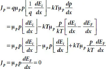
(1.6) 
Similarly, net current density for electrons is given as follows,
(1.7) 
(1.8) 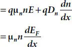
(1.9) 
Hence,
(1.10) 
It is apparent from equations (1.6)and (1.10)that the Fermi level ( E F) is not dependent on x and remains uniform in whole of the semiconductor sample for zero net hole and electron densities. This is also apparent from the band diagram as shown in Figure 1.6(b). A typical space charge distribution happens at the barrier due to uniform E Fin the steady state. Considering the 1D p-n junction when all donor and acceptor atoms are ionized, Poisson’s equation for electrostatic potential ψ and unique space charge distribution is given as follows [10,23,24],
(1.11) 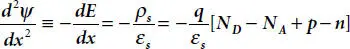
The above situation is well represented in Figure 1.9(a)in the energy band diagram of an abrupt junction in the steady state. There is a unique space charge distribution at the semiconductor junction. At distances far away from the barrier, net hole density is equal to the net electron density such that the total space charge density is zero maintaining the charge neutrality. In this case, from equation (1.11)[10,11,23,24],
(1.12) 
and,
(1.13) 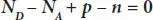
In case of a p -type neutral region, N D= 0 and p >> n . Now, setting N D= n = 0 in equation (1.13), we get, p = N Aand putting it in equation (1.3)[10,11,23,24],
(1.14) 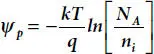
Figure 1.9 The above figure (a) displays band diagram of an abrupt junction in steady state and (b) displays an approximation of space charge distribution.
Similarly, in case of n -type neutral region, N A= 0 and n ≫ p Now, setting N A= p = 0 in equation (1.13), we get, n = N Dand putting in equation (1.3)[10,11,23,24],
(1.15) 
In the steady state, the total electrostatic potential difference between p -type and n -type neutral regions is defined as the built-in-potential ( V bi) and is given as follows [10,11,23,24],
(1.16) 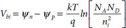
In between the neutral regions and semiconductor barrier, a narrow transition region exists which has a width smaller in comparison to the width of the barrier or the depletion region. This is true for regions existing on both sides of the depletion region. On neglecting the transition regions in comparison to the depletion region, a nearby rectangular space charge distribution is obtained as shown in Figure 1.9(b)[10,23,24]. Here, x pand x nare the widths of the depletion layer of p - and n -type blocks. In case of completely depleted region, the amount of p and n dopants will be zero, and then from equation (1.11)[10,24],
(1.11)
(1.17) 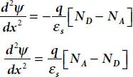
The physics of Poisson’s equation lies in the fact that distribution of impurities can be performed in the form of shallow diffusion or low energy ion implantation or in the form of deep diffusions or high-energy ion implantations [10,23,24]. The type of ion implantation describes the doping profile according to the energy dose applied [30]. Shallow diffusion or low-energy ion implantation introduces foreign atoms at low depths to form abrupt p-n junction as shown in Figure 1.10(a). In this case, the doping concentration profile shows a rapid changeover between the p -type and n -type regions. In case of high-energy ion implantations, distribution of doping profiles can be approximated almost linearly across the barrier called as linearly graded junction as shown in Figure 1.10(b).
Читать дальшеИнтервал:
Закладка:
Похожие книги на «Green Energy»
Представляем Вашему вниманию похожие книги на «Green Energy» списком для выбора. Мы отобрали схожую по названию и смыслу литературу в надежде предоставить читателям больше вариантов отыскать новые, интересные, ещё непрочитанные произведения.


Обсуждение, отзывы о книге «Green Energy» и просто собственные мнения читателей. Оставьте ваши комментарии, напишите, что Вы думаете о произведении, его смысле или главных героях. Укажите что конкретно понравилось, а что нет, и почему Вы так считаете.