Christopher Hallinan - Embedded Linux Primer - A Practical, Real-World Approach
Здесь есть возможность читать онлайн «Christopher Hallinan - Embedded Linux Primer - A Practical, Real-World Approach» весь текст электронной книги совершенно бесплатно (целиком полную версию без сокращений). В некоторых случаях можно слушать аудио, скачать через торрент в формате fb2 и присутствует краткое содержание. Год выпуска: 2006, ISBN: 2006, Издательство: Prentice Hall, Жанр: ОС и Сети, на английском языке. Описание произведения, (предисловие) а так же отзывы посетителей доступны на портале библиотеки ЛибКат.

- Название:Embedded Linux Primer: A Practical, Real-World Approach
- Автор:
- Издательство:Prentice Hall
- Жанр:
- Год:2006
- ISBN:978-0-13-167984-9
- Рейтинг книги:4 / 5. Голосов: 1
-
Избранное:Добавить в избранное
- Отзывы:
-
Ваша оценка:
Embedded Linux Primer: A Practical, Real-World Approach: краткое содержание, описание и аннотация
Предлагаем к чтению аннотацию, описание, краткое содержание или предисловие (зависит от того, что написал сам автор книги «Embedded Linux Primer: A Practical, Real-World Approach»). Если вы не нашли необходимую информацию о книге — напишите в комментариях, мы постараемся отыскать её.
This book brings together indispensable knowledge for building efficient, high-value, Linux-based embedded products: information that has never been assembled in one place before. Drawing on years of experience as an embedded Linux consultant and field application engineer, Christopher Hallinan offers solutions for the specific technical issues you're most likely to face, demonstrates how to build an effective embedded Linux environment, and shows how to use it as productively as possible.
Hallinan begins by touring a typical Linux-based embedded system, introducing key concepts and components, and calling attention to differences between Linux and traditional embedded environments. Writing from the embedded developer's viewpoint, he thoroughly addresses issues ranging from kernel building and initialization to bootloaders, device drivers to file systems.
Hallinan thoroughly covers the increasingly popular BusyBox utilities; presents a step-by-step walkthrough of porting Linux to custom boards; and introduces real-time configuration via CONFIG_RT--one of today's most exciting developments in embedded Linux. You'll find especially detailed coverage of using development tools to analyze and debug embedded systems--including the art of kernel debugging.
• Compare leading embedded Linux processors
• Understand the details of the Linux kernel initialization process
• Learn about the special role of bootloaders in embedded Linux systems, with specific emphasis on U-Boot
• Use embedded Linux file systems, including JFFS2--with detailed guidelines for building Flash-resident file system images
• Understand the Memory Technology Devices subsystem for flash (and other) memory devices
• Master gdb, KGDB, and hardware JTAG debugging
• Learn many tips and techniques for debugging within the Linux kernel
• Maximize your productivity in cross-development environments
• Prepare your entire development environment, including TFTP, DHCP, and NFS target servers
• Configure, build, and initialize BusyBox to support your unique requirements
Embedded Linux Primer: A Practical, Real-World Approach — читать онлайн бесплатно полную книгу (весь текст) целиком
Ниже представлен текст книги, разбитый по страницам. Система сохранения места последней прочитанной страницы, позволяет с удобством читать онлайн бесплатно книгу «Embedded Linux Primer: A Practical, Real-World Approach», без необходимости каждый раз заново искать на чём Вы остановились. Поставьте закладку, и сможете в любой момент перейти на страницу, на которой закончили чтение.
Интервал:
Закладка:
2.3.3. Flash Usage
An embedded system designer has many options in the layout and use of Flash memory. In the simplest of systems, in which resources are not overly constrained, raw binary data (perhaps compressed) can be stored on the Flash device. When booted, a file system image stored in Flash is read into a Linux ramdisk block device, mounted as a file system and accessed only from RAM. This is often a good design choice when the data in Flash rarely needs to be updated, and any data that does need to be updated is relatively small compared to the size of the ramdisk. It is important to realize that any changes to files in the ramdisk are lost upon reboot or power cycle.
Figure 2-4 illustrates a common Flash memory organization that is typical of a simple embedded system in which nonvolatile storage requirements of dynamic data are small and infrequent.
Figure 2-4. Example Flash memory layout

The bootloader is often placed in the top or bottom of the Flash memory array. Following the bootloader, space is allocated for the Linux kernel image and the ramdisk file system image, [8] We discuss ramdisk file systems in much detail in Chapter 9, "File Systems."
which holds the root file system. Typically, the Linux kernel and ramdisk file system images are compressed, and the bootloader handles the decompression task during the boot cycle.
For dynamic data that needs to be saved between reboots and power cycles, another small area of Flash can be dedicated, or another type of nonvolatile storage [9] Real-time clock modules often contain small amounts of nonvolatile storage, and Serial EEPROMs are another common choice for nonvolatile storage of small amounts of data.
can be used. This is a typical configuration for embedded systems with requirements to store configuration data, as might be found in a wireless access point aimed at the consumer market, for example.
2.3.4. Flash File Systems
The limitations of the simple Flash layout scheme described in the previous paragraphs can be overcome by using a Flash file system to manage data on the Flash device in a manner similar to how data is organized on a hard drive. Early implementations of file systems for Flash devices consisted of a simple block device layer that emulated the 512-byte sector layout of a common hard drive. These simple emulation layers allowed access to data in file format rather than unformatted bulk storage, but they had some performance limitations.
One of the first enhancements to Flash file systems was the incorporation of wear leveling. As discussed earlier, Flash blocks are subject to a finite write lifetime. Wear-leveling algorithms are used to distribute writes evenly over the physical erase blocks of the Flash memory.
Another limitation that arises from the Flash architecture is the risk of data loss during a power failure or premature shutdown. Consider that the Flash block sizes are relatively large and that average file sizes being written are often much smaller relative to the block size. You learned previously that Flash blocks must be written one block at a time. Therefore, to write a small 8KB file, you must erase and rewrite an entire Flash block, perhaps 64KB or 128KB in size; in the worst case, this can take tens of seconds to complete. This opens a significant window of risk of data loss due to power failure.
One of the more popular Flash file systems in use today is JFFS2, or Journaling Flash File System 2. It has several important features aimed at improving overall performance, increasing Flash lifetime, and reducing the risk of data loss in case of power failure. The more significant improvements in the latest JFFS2 file system include improved wear leveling, compression and decompression to squeeze more data into a given Flash size, and support for Linux hard links. We cover this in detail in Chapter 9, "File Systems," and again in Chapter 10, "MTD Subsystem," when we discuss the Memory Technology Device (MTD) subsystem.
2.3.5. Memory Space
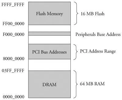
Virtually all legacy embedded operating systems view and manage system memory as a single large, flat address space. That is, a microprocessor's address space exists from 0 to the top of its physical address range. For example, if a microprocessor had 24 physical address lines, its top of memory would be 16MB. Therefore, its hexadecimal address would range from 0x00000000 to 0x00ffffff. Hardware designs commonly place DRAM starting at the bottom of the range, and Flash memory from the top down. Unused address ranges between the top of DRAM and bottom of FLASH would be allocated for addressing of various peripheral chips on the board. This design approach is often dictated by the choice of microprocessor. Figure 2-5 is an example of a typical memory layout for a simple embedded system.
Figure 2-5. Typical embedded system memory map
In traditional embedded systems based on legacy operating systems, the OS and all the tasks [10] In this discussion, the word task is used to denote any thread of execution, regardless of the mechanism used to spawn, manage, or schedule it.
had equal access rights to all resources in the system. A bug in one process could wipe out memory contents anywhere in the system, whether it belonged to itself, the OS, another task, or even a hardware register somewhere in the address space. Although this approach had simplicity as its most valuable characteristic, it led to bugs that could be difficult to diagnose.
High-performance microprocessors contain complex hardware engines called Memory Management Units (MMUs) whose purpose is to enable an operating system to exercise a high degree of management and control over its address space and the address space it allocates to processes. This control comes in two primary forms: access rights and memory translation. Access rights allow an operating system to assign specific memory-access privileges to specific tasks. Memory translation allows an operating system to virtualize its address space, which has many benefits.
The Linux kernel takes advantage of these hardware MMUs to create a virtual memory operating system. One of the biggest benefits of virtual memory is that it can make more efficient use of physical memory by presenting the appearance that the system has more memory than is physically present. The other benefit is that the kernel can enforce access rights to each range of system memory that it allocates to a task or process, to prevent one process from errantly accessing memory or other resources that belong to another process or to the kernel itself.
Let's look at some details of how this works. A tutorial on the complexities of virtual memory systems is beyond the scope of this book. [11] Many good books cover the details of virtual memory systems. See Section 2.5.1, "Suggestions for Additional Reading," at the end of this chapter, for recommendations.
Instead, we examine the ramifications of a virtual memory system as it appears to an embedded systems developer.
2.3.6. Execution Contexts
One of the very first chores that Linux performs when it begins to run is to configure the hardware memory management unit (MMU) on the processor and the data structures used to support it, and to enable address translation. When this step is complete, the kernel runs in its own virtual memory space. The virtual kernel address selected by the kernel developers in recent versions defaults to 0xC0000000. In most architectures, this is a configurable parameter. [12] However, there is seldom a good reason to change it.
If we were to look at the kernel's symbol table, we would find kernel symbols linked at an address starting with 0xC0xxxxxx. As a result, any time the kernel is executing code in kernel space, the instruction pointer of the processor will contain values in this range.
Интервал:
Закладка:
Похожие книги на «Embedded Linux Primer: A Practical, Real-World Approach»
Представляем Вашему вниманию похожие книги на «Embedded Linux Primer: A Practical, Real-World Approach» списком для выбора. Мы отобрали схожую по названию и смыслу литературу в надежде предоставить читателям больше вариантов отыскать новые, интересные, ещё непрочитанные произведения.


Обсуждение, отзывы о книге «Embedded Linux Primer: A Practical, Real-World Approach» и просто собственные мнения читателей. Оставьте ваши комментарии, напишите, что Вы думаете о произведении, его смысле или главных героях. Укажите что конкретно понравилось, а что нет, и почему Вы так считаете.