John Crisp - Introduction to Microprocessors and Microcontrollers
Здесь есть возможность читать онлайн «John Crisp - Introduction to Microprocessors and Microcontrollers» весь текст электронной книги совершенно бесплатно (целиком полную версию без сокращений). В некоторых случаях можно слушать аудио, скачать через торрент в формате fb2 и присутствует краткое содержание. Год выпуска: 2004, ISBN: 2004, Издательство: Elsevier, Жанр: Компьютерное железо, на английском языке. Описание произведения, (предисловие) а так же отзывы посетителей доступны на портале библиотеки ЛибКат.
- Название:Introduction to Microprocessors and Microcontrollers
- Автор:
- Издательство:Elsevier
- Жанр:
- Год:2004
- ISBN:0-7506-5989-0
- Рейтинг книги:3 / 5. Голосов: 1
-
Избранное:Добавить в избранное
- Отзывы:
-
Ваша оценка:
Introduction to Microprocessors and Microcontrollers: краткое содержание, описание и аннотация
Предлагаем к чтению аннотацию, описание, краткое содержание или предисловие (зависит от того, что написал сам автор книги «Introduction to Microprocessors and Microcontrollers»). Если вы не нашли необходимую информацию о книге — напишите в комментариях, мы постараемся отыскать её.
Introduction to Microprocessors and Microcontrollers — читать онлайн бесплатно полную книгу (весь текст) целиком
Ниже представлен текст книги, разбитый по страницам. Система сохранения места последней прочитанной страницы, позволяет с удобством читать онлайн бесплатно книгу «Introduction to Microprocessors and Microcontrollers», без необходимости каждый раз заново искать на чём Вы остановились. Поставьте закладку, и сможете в любой момент перейти на страницу, на которой закончили чтение.
Интервал:
Закладка:
Integer unit and registers
As expected with a RISC processor, there are plenty of registers. In this section of the 601, we have 32 registers, each 32-bits wide. These registers are dual-ported. This means that two circuits can access the registers at the same time without interfering with each other. This is like someone reading the back of your newspaper as you are reading the front – except that registers don’t find it irritating. ‘Port’, by the way, is just a fancy electronic word meaning ‘connection’. Transistors, generally, have three wires going to them and so are described as three-port devices.
The integer unit handles all instructions like integer arithmetic bit manipulation and transferring data to and from the external memory and is organized into a three-stage pipeline. In Figure 13.3, the second clock pulse executes the first instruction. The next clock pulse executes the second instruction and the last clock pulse executes the third. We have achieved the target of one clock pulse per clock pulse. And in the fourth clock pulse, we can see the next instruction just arriving to be decoded immediately after the first write-back.
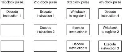
Figure 13.3 Integer unit pipeline
Floating-point unit
This has a further 32 registers but in this case, they are 64-bits wide and to fill a register with a single clock pulse, there is an internal 64-bit bus connecting it with the cache. The pipeline is five stage: prefetch, buffer, decode, execution and write-back.
Memory buffer
This acts as a buffer for the external memory. The buffers include two reads and three writes, each up to 32 bytes. It is also used in writing-back to the cache.
Big and little endians
The main memory is divided into locations each having its own address. Each location can hold a single byte of information. If we wanted to store a 32-bit number, then we would have to utilize four consecutive locations.
Imagine that we wished to store the 32-bit number 00000000 01010101 00010001 11111111 2and we had addresses 24646603H, 24646602H, 24646601H and 24646600H available. Little-endian format would store the most significant byte in the highest memory address so, in our example, the data 00000000 would go into address 24646603H. This is used by Intel microprocessors. Big-endian, which Motorola uses, works the other way around. The most significant byte is put in the lowest memory address so, in our example, the data 00000000 would go into address 24646600H. These are shown in Figure 13.4. All the PowerPC microprocessors are switchable to enable little or big-endian to be used.
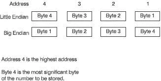
Figure 13.4 Big and little endians
A large number of PowerPCs have continued to power the Apple-Mac and IBM desktops and, in addition, support both the UNIX and Linux operating systems.
The latest offering is the 970 with its 52 million transistors started life as a 1.8 GHz device and has now progressed to 2.0 GHz. This may appear slow but it has compensating attributes such as its 900 MHz bus as opposed to the 533 MHz bus of the Pentium 4.
It is a 64-bit micro so it handles data in 64-bit chunks but remains compatible with earlier 32-bit designs. It has two level 1 caches, one for instructions at 64 kB and a data cache of 32 kB, which are somewhat larger that the Intel product but both companies use a level 2 cache of 512 kB.
As memory size is continuing to increase with each design, the size of memory that can be directly accessed increases with the move to 64-bit processing. The Pentium 4 can access 40 GB of memory, which seems excessively large at the moment but there was a time when 4 MB was something to wonder at. The PowerPC 970 can handle memory of Star Trek proportions measured in terabytes (thousands of Gigs).
Table 13.1 Cache sizes
| L1 Instruction | L1 Data | L2 cache | |
|---|---|---|---|
| PowerPC 970 | 64 kB | 32 kB | 512 kB |
| Pentium 4 | It’s a secret | 8 kB | 512 kB |
For maximum microprocessor speed we need a high clock speed combined with the maximum use being made of every part of the microprocessor. The early 8-bit microprocessors would accept the first instruction and it would pass through the microprocessor being decoded, then acted upon, then having the results stored before it considered the next instruction. This meant that each bit of the micro was doing nothing for much of the time.
Modern micros load many instructions at the same time and split up the tasks so that as many as possible can be carried out at the same time to have the minimum time wastage.
As with the Pentium 4, the PPC970 makes use of level 1 caches that, as is now common, are split into an Instruction cache and a Data cache. There is also a level 2 cache and an external level 3 cache.
Loading the instructions
The instructions pour down from the Instruction cache at a maximum rate of eight per cycle, though five is a more likely overall figure. But this is still fast.
The PP970 uses a very long pipeline and can be handling up to 200 instructions simultaneously. The price of such a long pipeline is that we must be careful to ensure that it is filled with the most useful instructions and hence we need to back it up with very effective branch prediction techniques.
Branch prediction
To obtain the maximum possible speed, the PP970 has devoted a great deal of resources into its branch prediction. As the instructions are loaded, the branch prediction circuitry scans the incoming instruction looking for branch instructions. Every time we meet a branch instruction that offers a choice of outcome the branch will have to be accepted or rejected.
The 970 has two branch prediction methods. The first is very similar to that used in the Pentium 4 and, to over simplify the situation, it follows the same sort of reasoning as we often adopt in everyday life. If it usually happens, it is most likely to happen again. The 970 keeps a record of the previous 16384 branches in its BHT (Branch History Table) to see how often each choice was made and then this information is further sorted by a prediction program before it comes to a final decision.
The second method involves a similar sized table called a Global Predictor. This method also comes up with a final go/no go for the branch but it decides by generating an 11-bit vector that stores the actual execution path taken by the previous eleven fetch groups leading up to the branch.
So there are two independent mechanisms that make a decision as to whether the branch should be taken. If they disagree, we need a referee. This job is performed by a ‘Selector Table’ that stores the success rate for each of the two previous methods for each particular branch. It then makes the final decision – and it is said (by IBM) to be very successful, which it probably is.
Handling the instructions
Having combined the incoming instruction stream from the Instruction cache with the information from the Branch predict, the instruction are queued and passed to the Decode, Crack and Group Formation Unit. At this stage, in order to keep the instruction handling speed at a maximum, this unit takes the instruction codes from the Instruction cache, decodes them and cracks them into their component parts called Internal Operations (IOPs). These very small but simple tasks are passed out to specialized units like the five blocks shown along the bottom of Figure 13.5.
Читать дальшеИнтервал:
Закладка:
Похожие книги на «Introduction to Microprocessors and Microcontrollers»
Представляем Вашему вниманию похожие книги на «Introduction to Microprocessors and Microcontrollers» списком для выбора. Мы отобрали схожую по названию и смыслу литературу в надежде предоставить читателям больше вариантов отыскать новые, интересные, ещё непрочитанные произведения.


Обсуждение, отзывы о книге «Introduction to Microprocessors and Microcontrollers» и просто собственные мнения читателей. Оставьте ваши комментарии, напишите, что Вы думаете о произведении, его смысле или главных героях. Укажите что конкретно понравилось, а что нет, и почему Вы так считаете.