Break
Session 2: Modelling of novel materials Сhairs: I. Bobrinetskiy /D. Krasnikov
11.45–12.10
Keynote Talk 3 Prof.Olga Glukhova
Anisotropic electrical conductivity in graphene films with vertically aligned single-walled carbon nanotubes: new advances in mechanisms and applications
12.10–12.35
Keynote Talk 4 Prof. Kari Laasonen
Oxygen evolution reaction on pristine and defective nitrogen-doped carbon nanotubes and graphene
12.35–12.50
Oral Talk 3: Prof. Stefan Shcherbinin
Starfish-like phosphorus carbide nanotubes
12.50–13.05
Oral Talk 4: Prof. Alexander Kvashnin
Computational search for new high-T Csuperconductors with subsequent synthesis
13.05–13.20
Sponsor talk (Swagelok)
13.20–14.40
Break/lunch time
Session 3: Electrochemistry of novel materials Сhairs: L. Bulusheva/ F. Fedorov
14.40–15.05
Keynote Talk 5 Prof. Keith Stevenson
Enhanced Electrocatalytic Activities by Substitutional Tuning of Nickel-based Ruddlesden-Popper Catalysts for the Oxidation of Urea and Small Alcohols
15.05–15.30
Keynote Talk 6 Prof. Carita Kvarnström
Electrochemical synthesis of copolymers containing porphyrine derivatives and their activity towards CO 2
15.30–15.45
Oral talk 5 Prof. Bernardo Barbiellini
Positronium emission from materials for Li-ion batteries
15.45–16.00
Oral Talk 6 Dr. Stanislav Evlashin
The role of nitrogen and oxygen in the formation capacity of carbon materials
16.00–16.25
Break
Session 3: Electrochemistry of novel materials Chairs: P. Lund / E. Fedorovskaya
16.25–16.50
Keynote Talk 9 Prof. Cristina Flox
Nickel-Nitrogen active sites towards selective High-rate CO2-to-formate electroreduction
16.50–17.15
Keynote Talk 10 Prof. Jari Koskinen
Development of materials for electrochemical bio-sensing
17.15–17.30
Oral Talk 7 Dr. Stanislav Fedotov
Defects in olivine-type cathode materials for Li-ion batteries
17.30–17.45
Oral talk 8 Dr. Muhammad Asghar
Ceramic fuel cell fabrication trend from conventional methods to digital printing

Structure of graphitized films formed on the diamond surface under high-temperature annealing
A.V. Okotrub 1, D.V. Gorodetskii 1, Y.N. Palyanov 2, A.L. Chuvilin 3, L.G. Bulusheva 1
1 – Nikolaev Institute of Inorganic Chemistry, SB RAS, 630090 Novosibirsk, Russia
2 – Sobolev Institute of Geology and Mineralogy SB RAS, 630090 Novosibirsk, Russia
3 – CIC nanoGUNE Consolider, E-20018 San Sebastian, Spain
spectrum@niic.nsc.ru
Diamond crystals with a facet size exceeding the size of the focus of the X-ray beam incident on the sample were synthesized by the HPHT method were heated to a temperature of 850 °C and 1250 °C for 15 minutes. Annealing of samples of single crystals was carried out in a high-vacuum chamber of the Russian-German laboratory at the BESSY II synchrotron source. XPS spectroscopy was used to study the structure of carbon layers on diamond faces of different symmetries and with thin layers of iron and nickel deposited on a diamond. A higher rate of graphitization of the (111) face is shown. From the data of the angular dependence of NEXAFS, the directionality of the sp 2carbon layers relative to the diamond surface is determined. The data obtained indicate a catalytic effect of the metal on the process of the formation of graphene structures. Transmission electron microscopy data demonstrate the characteristic size and misorientation of individual graphene layers for different symmetry of diamond faces.
Acknowledgement.This work was supported by the Russian Foundation for Basic Research, grant 19-03-00425.
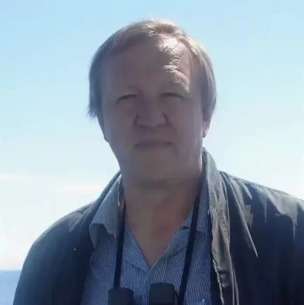
Prof. Dr. Alexander Okotrub

Alexander Okotrub graduated from the Physics Department of Novosibirsk State University in 1980, specialized in the Chemical Physics. Since 1980, A. Okotrub worked as an intern-researcher at Nikolaev Institute of Inorganic Chemistry SB RAS (NIIC SB RAS) as post-graduate student, junior researcher, research associate, senior researcher, leading researcher and principal researcher. At present he is the head of the Laboratory of Physics Chemistry of Nanomaterials and the head of the Department of the Chemistry of Functional Materials of the NIIC SB RAS. He is professor in physical chemistry and leads the Laboratory of Carbon Nanomaterials at the Novosibirsk State University. In his work, an approach is used that combines methods for synthesizing carbon nanostructures (fullerenes, nanotubes, graphene, nanodiamonds, etc.), methods for their chemical modification and the creation of composite and hybrid structures, as well as methods for studying the structure and physicochemical properties of the produced materials. Considerable attention is paid to X-ray and photoelectron spectroscopy and quantum-chemical calculations for studying the electronic structure and properties of new materials. A. Okotrub published 360 scientific papers. He lectures on "Functional materials" for students of the Novosibirsk State University and "Materials and their properties" for post-graduate students of the NIIC SB RAS.
FC–CVD synthesis large diameter CNTs for transparent conductor applications
Qiang Zhang, Datta Sukanta, Hua Jiang, Esko I. Kauppinen
Department of Applied Physics, Aalto University School of Science, PO Box 15100, FI-00076 Aalto, Espoo, FINLAND
esko.kauppinen@aalto.fi
Many efforts have been devoted to increasing the conductivity of CNT TCFs made with the floating catalyst chemical vapor deposition (FC–CVD). However, intrinsic nanotube collisions in the aerosol process of FC–CVD lead to a tread-off between yield and performance, because bundling increases when increasing the yield i.e. production rate, with the bundling reducing the growth rate as well as increasing sheet resistance at the given film transmittance. Here, we report TCFs of large-diameter CNTs from methane-based FC–CVD overcoming the performance-yield tradeoff. Based on the Fe-C-S system, the double-wall CNTs (DWCNTs) with a mean diameter of 4.15 nm and a mean bundle length of 20 um have been synthesized via FC–CVD and directly deposited to form TCFs. After gold chloride solution doping, the TCFs have an excellent performance of 42 ohm/sq sheet resistance at 90 % transmittance. Unexpectedly, these high-performance DWCNTs films have an ultra-high yield i.e. production rate, being two orders of magnitude higher than that of SWCNT based TCFs with similar performance. Especially, these high-yield DWCNTs films contain ‘small’ bundles with around 50 % of CNTs being individual, which is completely different from other FC–CVD results for SWCNTs produced at much lower yield. Moreover, the large-diameter DWCNTs seem to flatten at the junctions, which may provide a larger contact area between the tubes and accordingly reduce the contact resistance. These unique features of large-diameter CNTs in ‘small’ bundles offer the route to obtain high-performance CNT TCFs with high yield. These results imply a new model with optimization windows for high-performance CNT TCFs with high yields and accordingly at reduced cost, and may accelerate the practical application of CNTs TCFs.
Читать дальше
