Chris Binns - Introduction to Nanoscience and Nanotechnology
Здесь есть возможность читать онлайн «Chris Binns - Introduction to Nanoscience and Nanotechnology» — ознакомительный отрывок электронной книги совершенно бесплатно, а после прочтения отрывка купить полную версию. В некоторых случаях можно слушать аудио, скачать через торрент в формате fb2 и присутствует краткое содержание. Жанр: unrecognised, на английском языке. Описание произведения, (предисловие) а так же отзывы посетителей доступны на портале библиотеки ЛибКат.
- Название:Introduction to Nanoscience and Nanotechnology
- Автор:
- Жанр:
- Год:неизвестен
- ISBN:нет данных
- Рейтинг книги:4 / 5. Голосов: 2
-
Избранное:Добавить в избранное
- Отзывы:
-
Ваша оценка:
Introduction to Nanoscience and Nanotechnology: краткое содержание, описание и аннотация
Предлагаем к чтению аннотацию, описание, краткое содержание или предисловие (зависит от того, что написал сам автор книги «Introduction to Nanoscience and Nanotechnology»). Если вы не нашли необходимую информацию о книге — напишите в комментариях, мы постараемся отыскать её.
Introduction to Nanoscience and Nanotechnology — читать онлайн ознакомительный отрывок
Ниже представлен текст книги, разбитый по страницам. Система сохранения места последней прочитанной страницы, позволяет с удобством читать онлайн бесплатно книгу «Introduction to Nanoscience and Nanotechnology», без необходимости каждый раз заново искать на чём Вы остановились. Поставьте закладку, и сможете в любой момент перейти на страницу, на которой закончили чтение.
Интервал:
Закладка:
The aspect of incremental nanotechnology that has really changed in the modern world is the development of instruments (see Chapter 5) that can probe at the nanoscale and image the particles within materials or devices. Researchers can actually observe what is happening to the particles or grains in response to changes in processing. This not only makes development of new processes more efficient, but also leads to the discovery of completely new structures that were not known to exist and hence new applications. Nature is full of surprises when one studies sufficiently, small pieces of matter, as will be come clear throughout this book.
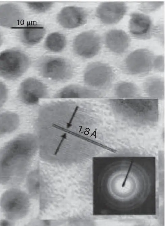
Figure I.2 Ancient incremental nanotechnology.Copper nanocrystals of about 10 nm in diameter on a tenth century pot, which produce a surface luster. The inset shows an increased magnification image of a single 7 nm diameter particle with atomic planes visible revealing its crystallinity.
Source: Reproduced with permission from [3].
I.2 Evolutionary Nanotechnology
Whereas Incremental Nanotechnology is the business of assembling vast numbers of very tiny particles to produce novel substances, Evolutionary Nanotechnology attempts to produce nanoparticles that individually perform some kind of useful function. They may need to be assembled in vast numbers to form a macroscopic array in order to build a device, but a functionality is built into each one. Such nanoparticles are necessarily more complex than those used in incremental nanotechnology, and will often consist of more than one material and have a surface coating of organic molecules.
An example of a single nanoparticle device is a single‐electron transistor (SET), that uses a phenomenon known as “Coulomb blockade” to effect transistor action on individual electrons (see Chapter 6). The device works in a similar manner to a field effect transistor (FET), that is, it is conducting or not conducting through the main terminals depending upon the value of a voltage applied to a third “gate” electrode. The difference is that the “on” and “off” states control single electrons hopping through the device, and the action is carried out by a single nanoparticle a few nanometers across. The smallest device that has exhibited transistor action this way is a 66‐atom aluminium nanoparticle with a diameter of about 1.5 nm [4].
The research has so far only provided proof‐of‐principle of transistor action either by finding a clever scheme to address a single nanoparticle with relatively large electrodes as illustrated in Figure I.7, or by investigating a large number of identical particles at once. The problem of how to interconnect the individual nanoparticles among themselves to form a circuit and communicate with them at the nanoscale has yet to be solved. A possibility is to use molecular wires, and it has been shown that hydrocarbon chain molecules known as thiols, shown in Figure I.3a can act as conducting wires. These form particularly strong bonds to gold nanoparticles via the sulphur atom at one end and their resistance varies according to the length of the hydrocarbon chain and the nature of any end groups attached to the molecule. Thus, there is the possibility of molecular interconnections between nanoparticles.
To illustrate the state‐of‐play consider Figure I.3b, which shows a gold nanoparticle of about 3 nm diameter with thiols attached, which can be considered as an SET. The circuit diagram for an AND gate, a fundamental component of a computer logic circuit, implemented by three FETs is shown in Figure I.3c. The circuit with the FETs implemented by three Au nanoparticles SETs is shown in Figure I.3d with the dashed lines showing the connections that we are currently unable to make. Also, included are the power electrodes drawn to scale for the current state‐of‐the‐art minimum feature size (the “process size”) of 5 nm used in the semiconductor industry. This makes the whole gate about 32 nm across as compared to the equivalent using conventional “top–down” processing (see below) of about 260 nm ( Figure I.3e).
Thus, in terms of a real density, there is a factor of 50 to go in the miniaturization of circuits by exploiting nanoparticles. For this technology to come of age it is likely that some sort of self‐assembly of the thiol‐coated nanoparticles will be required, and so it is possible that devices like this could be grown chemically as illustrated in Figure I.4rather than “cut into” silicon. There are other schemes for individual nanoscale transistors based on carbon nanotubes and graphene discussed in Chapter 6, which focuses on single nanoparticle devices. These give about the same level of miniaturization, but the nanoscale interconnections present the same problems.
It is worth pointing out that for devices this small in which quantum effects start to become dominant, it might be more sensible to design the device as a quantum computer rather than a very small processor based on traditional logic gates. Quantum computers are beyond the scope of this book but are able to run, at least some algorithms, at an immensely higher speed than conventional computers. The main point of this example is to illustrate evolutionary nanotechnology where a single nanoparticle performs a function.
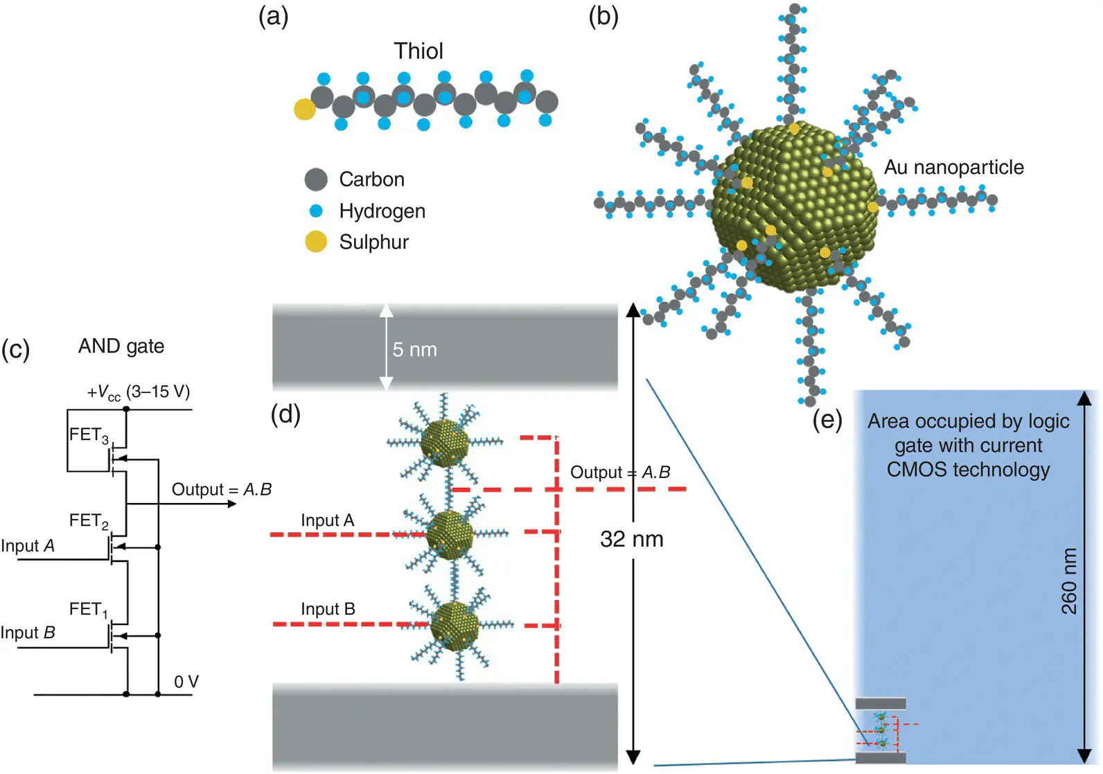
Figure I.3 Evolutionary nanotechnology – a single nanoparticle acting as a device.(a) A thiol hydrocarbon chain that can act as a “molecular wire”. (b) A gold nanoparticle with thiols attached, which can act as a SET that replicates the action of a conventional FET but for single electrons. (c) A circuit for an AND gate of a processor composed of three FETs. (d) The AND gate circuit implemented with nanoparticle SETs. The outer electrodes are drawn to scale for the smallest process size available with current semiconductor technology and the red dashed lines show the connections that we are currently unable to make. (e) The nanoparticle gate in comparison to the area occupied by an AND gate produced by current state‐of‐the‐art CMOS technology.
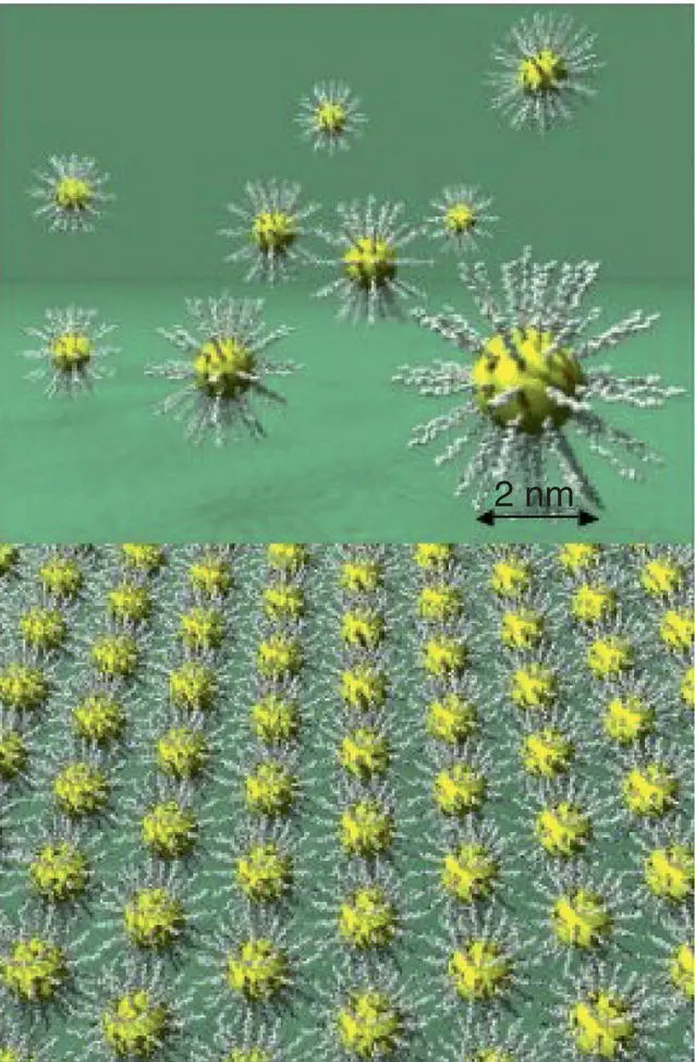
Figure I.4 Self‐assembly of single‐nanoparticle transistors.Illustration of gold nanoparticle transistors with attached thiols self‐assembling to form a circuit.
Source: Reproduced with the permission of Dr. Mark Everard from [5].
No one can fail to be impressed by the huge increases in performance, and density of components/memory elements in devices made by the electronics and magnetic recording industries in the last few decades. The above example illustrates, however, that there is still a long way to go, nicely reinforcing a lecture on nanotechnology given by the visionary Nobel Laureate Richard Feynman in 1959 entitled There's Plenty of Room at the Bottom . It is remarkable to note that this vision of nanotechnology was expounded over 60 years ago.
A more sophisticated example of an individual nanoparticle being able to perform useful tasks is illustrated in Figure I.5. Using a gas‐phase nanoparticle synthesis technology described in Chapter 5, it is possible to build nanoparticles starting with a core and then adding shells to make “nano‐onions” as demonstrated in Figure I.5a. This shows an electron microscope image of a Au@Ag@Co nanoparticle with a diameter of 8.5 nm, and the terminology denotes that the particle has a cobalt core coated with a silver shell and a second shell of gold. The elemental detection line scan using X‐ray fluorescence (see Chapter 5, Section 5.4.7) through the particle along the red line clearly shows the separation of the three elements. Using the same synthesis methods, it is also possible to prepare dumbbell or double nanoparticles as shown in Figure I.5b. These can either be of different elements, often referred to as Janus particles, with the name derived from the Roman god with two faces looking in opposite directions, or the same element.
Читать дальшеИнтервал:
Закладка:
Похожие книги на «Introduction to Nanoscience and Nanotechnology»
Представляем Вашему вниманию похожие книги на «Introduction to Nanoscience and Nanotechnology» списком для выбора. Мы отобрали схожую по названию и смыслу литературу в надежде предоставить читателям больше вариантов отыскать новые, интересные, ещё непрочитанные произведения.


Обсуждение, отзывы о книге «Introduction to Nanoscience and Nanotechnology» и просто собственные мнения читателей. Оставьте ваши комментарии, напишите, что Вы думаете о произведении, его смысле или главных героях. Укажите что конкретно понравилось, а что нет, и почему Вы так считаете.